Electronics · Ch 3 — Transistor Amplifiers
DC and AC equivalent circuit of amplifiers
DC and AC equivalent circuit of amplifiers
In a working transistor amplifier, direct current from the biasing supply and alternating current from the signal being amplified flow through the same components at the same time. To study such a circuit cleanly, its analysis is split into two independent parts — a DC analysis that fixes the transistor's operating point, and an AC analysis that gives its signal (small-signal) performance. Mastering both equivalent circuits is essential for the Karnataka 2nd PUC Electronics board exam, so work through each one carefully.
DC analysis and the DC equivalent circuit
DC analysis considers only the DC sources and finds the steady voltages and currents that set the operating point. The DC equivalent circuit is obtained in two steps:
- Reduce every AC source to zero.
- Open-circuit every capacitor, because a capacitor blocks DC.
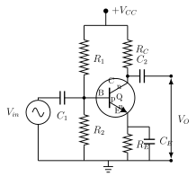
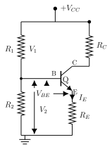
Applying this to the voltage-divider-biased CE amplifier of Figure 3.4.1 gives the DC equivalent of Figure 3.4.2. The supply divides across R1 and R2, and the voltage developed across R2 forward-biases the base–emitter junction. Writing Kirchhoff's voltage law (KVL) around the base–emitter loop gives the emitter current , and KVL around the collector–emitter loop relates the supply to . From these relations every DC voltage and current in the amplifier can be calculated.
The textbook prints the base–emitter loop as . For its own quoted result to follow, the loop must actually read — the divider voltage across R2 equals the base–emitter drop plus the drop across the emitter resistor. Treat the printed minus sign as a sign misprint and use the "+" form (as captured in the formula card below) when solving numerical problems.
AC analysis and the AC equivalent circuit (the re' model)
AC analysis finds how the amplifier responds to the signal alone. Its equivalent circuit is drawn in two steps:
- Replace every DC source by a short circuit.
- Replace every capacitor by a short circuit (at signal frequencies the coupling and bypass capacitors behave as shorts).
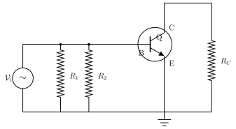
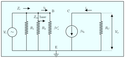
The first step gives Figure 3.4.3, in which R1 and R2 appear in parallel across the input and RC is the collector load. The second step replaces the transistor by its small-signal model, giving Figure 3.4.4, the re' model: the emitter–base junction is replaced by an AC resistance and the collector–base junction by a constant-current source. For a small AC signal the emitter diode does not rectify — it simply offers an AC resistance — while the collector diode behaves as a current source.
From the re' model, the section derives five performance quantities of the CE amplifier:
- Input impedance — the ratio of input voltage to input current. It is the parallel combination of the two bias resistors and the impedance looking into the base, and the impedance looking into the base works out to , where is the AC emitter-junction resistance. …
Drawn by us to help you understand the concept clearly, and verified to make sure it's accurate. For exams, practice from your textbook's own diagram.
Figure 3.4.1 — the complete CE amplifier: supply +Vcc, base voltage-divider R1–R2, collector resistor RC, emitter resistor RE with bypass capacitor CE, input coupling capacitor C1 and output coupling capacitor C2, driven by the AC source Vin. This is the starting circuit from which the DC equivalent (Figure 3.4.2) and …
Drawn by us to help you understand the concept clearly, and verified to make sure it's accurate. For exams, practice from your textbook's own diagram.
Figure 3.4.2 — with every capacitor opened and the AC source set to zero, only the DC bias path survives: the supply Vcc divides across R1 (drop V1) and R2 (drop V2), VBE is the base–emitter drop, and the emitter current IE flows through RE to ground. This circuit sets the transistor's operating poi …
Drawn by us to help you understand the concept clearly, and verified to make sure it's accurate. For exams, practice from your textbook's own diagram.
Figure 3.4.3 — shorting the DC supply and all capacitors places R1 and R2 in parallel across the input and grounds the emitter for AC, leaving RC as the collector load. This is the intermediate step, drawn before the transistor itse …
Drawn by us to help you understand the concept clearly, and verified to make sure it's accurate. For exams, practice from your textbook's own diagram.
Figure 3.4.4 — the re' model. The emitter–base junction is replaced by the AC resistance , into which the base current ib flows, and the collector–base junction by a constant-current source feeding the collector load RC. The input impedance Zi and the impedance looking into the base are marked. Every gain and impedan …
Voltage across R2 (forward-biases the base–emitter junction):
Emitter current from the base–emitter loop (using the corrected ):
…
Input impedance (ratio of input voltage to input current):
Impedance looking into the base:
AC emitter-junction resistance, with (silicon) and (germanium):
Output impedance: …
Voltage gain (the negative sign is the 180° phase reversal):
Current gain: …