Electronics · Ch 3 — Transistor Amplifiers
Multistage amplifier
Multistage amplifier
Very often the voltage gain, power amplification or frequency response available from a single stage of amplification is not enough to drive the load or to build up a strong enough signal. Two or more additional stages are then connected one after another — cascaded — to achieve greater voltage or current amplification, or both. In practice an amplifier is almost always multistage: a radio receiver, for example, may use six or more stages. Any circuit containing more than two stages of amplification is called a multistage amplifier, and its basic purpose is to increase the overall gain. This topic is a standing favourite in the II PUC board exam, so it is worth understanding the gain arithmetic and the three coupling methods in detail.
Multistage amplifiers fall into two categories:
- Compound amplifiers — the stages may differ from one another (one may be common-base, another common-collector) and different types of inter-stage coupling may be used.
- Cascaded amplifiers — every stage, and the coupling between stages, is identical: identical single-stage amplifiers connected in cascade, with the output of one stage feeding the input of the next.
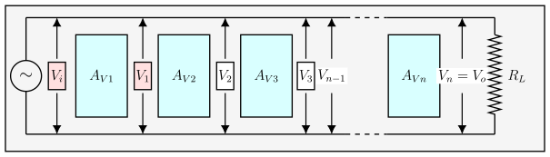
Need for cascading: because the gain of a single stage is not sufficient for practical applications, two or more stages are cascaded to build up a greater signal (Figure 3.6.1).
Overall gain of a multistage amplifier
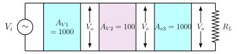
The overall voltage gain of a multistage amplifier is the product of the individual stage gains. When gains are expressed in decibels, the overall gain is instead the sum of the individual decibel gains — which is one reason gain is so often quoted in dB. For the three-stage example of Figure 3.6.2, with stage gains 1000, 100 and 1000, the overall gain is , which on the dB scale is .
Types of coupling in amplifiers
Coupling transfers the output of one stage to the input of the next. Three types are used:
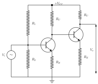
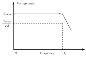
1. Direct coupled amplifier (Figure 3.6.3) — the output of one stage is connected directly to the input of the next, with no coupling components. It is used where the load must be connected directly to the output (headphones, loudspeakers), where the DC output current does not disturb the load, and it is suitable for uniform amplification of DC and very-low-frequency AC signals.
2. RC coupled amplifier (Figure 3.6.4) — the output of one stage is connected to the input of the next through a resistor and a capacitor. It provides higher voltage gain and higher overall amplification than the other methods, and because it uses no coils or transformers there are no magnetic fields to pick up undesirable signals, so non-linear distortion is minimum. It is used for amplifying audio-frequency (AF) signals.
3. Transformer coupled amplifier (Figure 3.6.5) — the output of one stage is coupled to the next through a transformer. Because a transformer is frequency-sensitive its frequency response is poor and its frequency range is limited; it is costly and bulky (heavy iron core) and tends to introduce a humming sound because its coils can pick up stray signals. Transformer coupling is normally used only in the last stage, where the aim is to maximise power transfer by impedance matching to a low-impedance load — for example a loudspeaker whose impedance is only 4 Ω to 16 Ω, against a transistor stage output impedance of several hundred ohms.
Two-stage R-C coupled transistor amplifier
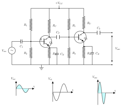
The R-C coupled amplifier is the most popular type because it gives excellent audio fidelity over a wide frequency range. Figure 3.6.6 shows a two-stage RC-coupled amplifier in CE configuration with voltage-divider bias. The coupling capacitor Cc joins the collector of the first stage to the base of the second; C1 couples the input signal into the first base and C2 couples the signal out of the last collector; R1, R2, RC and RE are the bias resistors, with RE providing stabilisation and CE bypassing AC across RE. Because each stage is coupled to the next by a series coupling capacitor followed by a shunt resistor, the circuit is called a resistance–capacitance coupled amplifier.
Working: an AC signal applied to the first stage is amplified and appears at its output with a 180° phase reversal. Cc feeds this signal to the second stage while blocking the DC bias of one stage from affecting the other. The second stage amplifies again with a further 180° reversal, so the final output is in phase with the input (the signal has been reversed twice). The overall voltage gain is the product of the two stage gains.
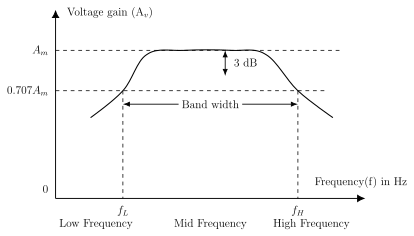
Frequency response (Figure 3.6.7): the voltage gain is small at low frequencies and at high frequencies and stays almost constant in the mid-frequency band. At low frequencies Cc offers a high reactance and passes only a small part of the signal, reducing the gain; at high frequencies Cc offers a low reactance and acts nearly as a short, increasing the loading of the next stage and reducing the gain. In the mid-band these two effects cancel and the gain stays constant. The bandwidth is the difference between the upper and lower cut-off frequencies, measured at the 0.707 (3 dB) points.
Advantages: cheap (only resistors and capacitors); good frequency response with uniform gain, so frequency distortion is low; minimum amplitude distortion (class-A operation, no coils/transformers); high overall gain compared with other couplings.
Disadvantages: the gain is comparatively small once loading of successive stages is taken into account; impedance matching is poor (high output impedance, low input impedance), so it cannot be used in the final stage against a loudspeaker; it becomes noisy with age and in moist climates; it cannot amplify DC or very-low-frequency signals; and power consumption is high because of the many resistors.
Applications: the initial (voltage-amplifier) stages of audio small-signal amplifiers such as radio receivers, TV receivers and public-address systems, because of its good frequency response.
Direct coupled transistor amplifier …
Drawn by us to help you understand the concept clearly, and verified to make sure it's accurate. For exams, practice from your textbook's own diagram.
Figure 3.6.1 — the input source Vi drives a chain of cascaded voltage-gain blocks AV1, AV2, AV3, …, AVn, with the inter-stage signal voltages V1, V2, V3, … marked, and the final stage delivering the output across the load Ri. It illustrates why stages are cascaded — to b …
Overall voltage gain = product of the individual stage gains:
In decibels, the overall gain = sum of the individual decibel gains:
…
Drawn by us to help you understand the concept clearly, and verified to make sure it's accurate. For exams, practice from your textbook's own diagram.
Figure 3.6.2 — three cascaded gain blocks (AV1 = 1000, AV2 = 100, AV3 = 1000) driven by Vi and feeding the load RL. The overall gain is , i.e. $20\l …

Drawn by us to help you understand the concept clearly, and verified to make sure it's accurate. For exams, practice from your textbook's own diagram.
Figure 3.6.3 — three amplifier blocks A1, A2, A3 in series with the output of one connected directly to the input of the next (no capacitors or transformers between stages). Direct coupling suits …

Drawn by us to help you understand the concept clearly, and verified to make sure it's accurate. For exams, practice from your textbook's own diagram.
Figure 3.6.4 — three amplifier blocks with each inter-stage link made by a series coupling capacitor C and a shunt resistor R, the last feeding the load RL. This resistor–capacitor coupling gives the RC-coupled ampli …

Drawn by us to help you understand the concept clearly, and verified to make sure it's accurate. For exams, practice from your textbook's own diagram.
Figure 3.6.5 — three amplifier blocks coupled by transformers between stages and feeding the output load RL. Transformer coupling is chiefly used in the final stage for impedance matching to a low-i …
Drawn by us to help you understand the concept clearly, and verified to make sure it's accurate. For exams, practice from your textbook's own diagram.
Figure 3.6.6 — two CE stages with voltage-divider bias. The input Viac enters through C1; coupling capacitor Cc links the first collector to the second base; C2 delivers the output Voac. Each stage has its own R1, R2, RC, RE and bypass CE. The waveforms below show the input, the inverted output of the first stage, and the final output th …
Drawn by us to help you understand the concept clearly, and verified to make sure it's accurate. For exams, practice from your textbook's own diagram.
Figure 3.6.7 — voltage gain versus frequency for an RC-coupled amplifier. The gain rises from low frequency, flattens at the mid-band value Am, then rolls off at high frequency; the lower and upper cut-off frequencies fL and fH are marked at the 0.707 Am (3 dB) level, and the bandwidth is the span betwee …
Drawn by us to help you understand the concept clearly, and verified to make sure it's accurate. For exams, practice from your textbook's own diagram.
Figure 3.6.8 — a two-stage direct-coupled amplifier: the collector of the first npn transistor connects directly (no coupling capacitor) to the base of the second, and the second collector drives the output vo. R1–R2 provide divider bias for the first transistor and bias the second indirectly, with RC and RE completing the bias. (The textbook caption print …
Drawn by us to help you understand the concept clearly, and verified to make sure it's accurate. For exams, practice from your textbook's own diagram.
Figure 3.6.9 — the frequency response of a direct-coupled amplifier: because there is no coupling capacitor, the gain stays constant at Av(max) from DC and low frequencies, falling only above the high-frequency cu …
| Particular | RC Coupling | Transformer Coupling | Direct Coupling |
|---|---|---|---|
| Frequency response | Excellent in the audio frequency range | Poor | Best |
| Cost | Less | More | Least |
| Space and weight | Less | More | Least |
| Impedance matching | Not good | Excellent | Good |