Electronics · Ch 3 — Transistor Amplifiers
Power Amplifiers
Power Amplifiers
A small-signal amplifier is essentially a voltage amplifier — it turns a small input voltage into a much larger output voltage but can deliver very little power. When an amplifier must instead drive a motor or feed a loudspeaker, where large switching currents are needed, a power amplifier is required.
A power (large-signal) amplifier boosts the power level of the input signal and delivers that amplified power to the load. It works by converting DC power drawn from the supply into an AC voltage signal at the load — in effect it is a DC-to-AC power converter whose action is controlled by the input signal. This conversion is never perfect: some power is always lost as heat and the amplifier itself consumes power, so the efficiency is usually poor even though an ideal amplifier would reach 100%. Efficiency is the ratio of the AC power delivered to the load to the DC power taken from the supply.
Voltage amplifier versus power amplifier
A voltage amplifier is designed for the largest possible voltage gain and draws little output power. A power amplifier instead feeds a large amount of power to the load, and to obtain that output power its input-signal voltage must itself be large — which is why, in a practical electronic system, a voltage amplifier always precedes the power amplifier.
Classification of power amplifiers
Power amplifiers are classified into four groups by the portion of the input cycle over which output (collector) current flows, which in turn is set by the position of the operating (Q) point:
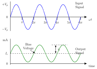
- Class A — Q-point at the centre of the linear amplifying region; output current flows for the full 360° cycle.
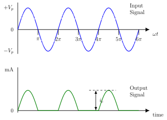
- Class B — Q-point at the cut-off region; output current flows for only half (180°) of the cycle.
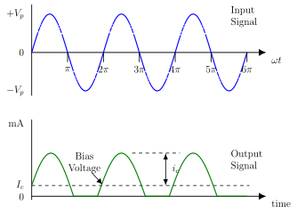
- Class AB — Q-point between the x-axis and the centre of the load line; output current flows for more than half but less than the full cycle.
- Class C — Q-point beyond cut-off (below the x-axis); output current flows for less than half of the cycle.
The input and output waveforms of the Class A, Class B and Class AB stages are shown in Figures 3.5.1, 3.5.2 and 3.5.3: the Class A output reproduces the whole cycle about the bias current level, the Class B output shows only the positive half-cycle humps, and the Class AB output conducts for a little more than a half-cycle with a small bias current.
Class B push–pull amplifier
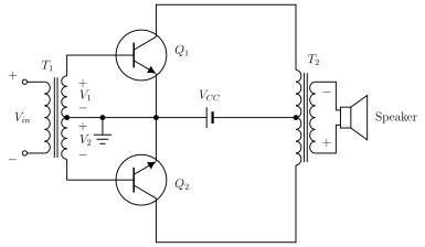
The transformer-coupled Class B push–pull amplifier (Figure 3.5.4) uses two centre-tapped transformers, T1 and T2, and two identical transistors Q1 and Q2. The input transformer T1 acts as a phase splitter, producing two drive voltages V1 and V2 that are 180° out of phase; the output transformer T2 couples the amplified signal from the collectors to the loudspeaker. Both transistors are biased at cut-off by giving them zero bias (base and emitter terminals joined); for balance, the two emitters connect to the centre tap of T1's secondary and Vcc connects to the centre tap of T2's secondary.
Working: on the positive half-cycle the upper transistor Q1 conducts while Q2 is cut off, and Q1's collector current is coupled through T2 to the loudspeaker as an amplified, inverted signal. On the negative half-cycle the polarities reverse, so Q2 turns on and Q1 turns off, and Q2 amplifies the other half. Because each transistor amplifies one half of the input, the loudspeaker receives a complete amplified cycle. The power efficiency is the AC output power divided by the DC input power.
Cross-over distortion
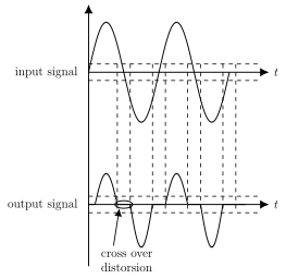
A transistor does not begin to conduct until the input signal voltage exceeds about 0.7 V for silicon or 0.3 V for germanium. In a push–pull stage this leaves a short interval near each zero crossing, between the positive and negative alternations, when neither transistor is conducting. The flattening of the output during this dead interval is called cross-over distortion (Figure 3.5.5).
Class C collector-tuned power amplifier
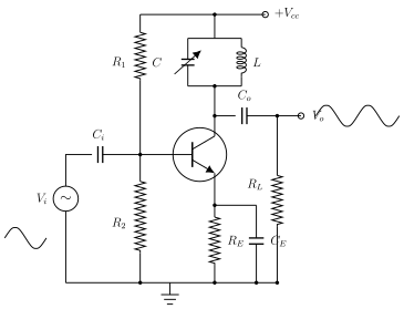
A single-tuned Class C power amplifier uses a parallel LC (tuned) circuit as its collector load (Figure 3.5.6). The inductance and capacitance are chosen so the circuit resonates at the frequency to be amplified, and the output is taken through a coupling capacitor. …
Efficiency is the AC power delivered to the load divided by the DC power taken from the supply:
For both the Class B push–pull and the Class C tuned amplifier this reads: …
Drawn by us to help you understand the concept clearly, and verified to make sure it's accurate. For exams, practice from your textbook's own diagram.
Figure 3.5.1 — a continuous sinusoidal input and, below it, the output collector current oscillating as a full sine wave about the bias-current level Ic. It conducts for the complete 360° cycle, which is the …
Drawn by us to help you understand the concept clearly, and verified to make sure it's accurate. For exams, practice from your textbook's own diagram.
Figure 3.5.2 — the same sinusoidal input, but the output appears only as separated positive half-cycle humps with the negative halves clipped to zero. A Class B stage conducts for onl …
Drawn by us to help you understand the concept clearly, and verified to make sure it's accurate. For exams, practice from your textbook's own diagram.
Figure 3.5.3 — the output humps are wider than in Class B and sit on a small Ic bias level, so the stage conducts for more than half but less than the full cycle. Class AB is the compromise between the low distortion of Class …
Drawn by us to help you understand the concept clearly, and verified to make sure it's accurate. For exams, practice from your textbook's own diagram.
Figure 3.5.4 — input source Vin feeds the centre-tapped phase-splitter transformer T1, whose secondary produces the 180°-out-of-phase voltages V1 and V2 that drive transistors Q1 and Q2. The collectors feed the centre-tapped output transformer T2 (Vcc at its centre tap), whose secondary drives the loudspeaker. …
Drawn by us to help you understand the concept clearly, and verified to make sure it's accurate. For exams, practice from your textbook's own diagram.
Figure 3.5.5 — the input sine (with the narrow ±0.7 V / ±0.3 V conduction-threshold band marked) above the distorted output. Near each zero crossing, where neither transistor is conducting, the output is flattened; the …
Drawn by us to help you understand the concept clearly, and verified to make sure it's accurate. For exams, practice from your textbook's own diagram.
Figure 3.5.6 — a parallel LC circuit (variable capacitor C in parallel with inductor L) forms the collector load, tuned to the signal frequency. The input signal Vi is coupled through Ci to the base (bias divider R1–R2, emitter RE with bypass CE), and the amplified output Vo is taken through coupling capacitor Co across the load RL. At resonance the tu …
| Class | A | B | C | AB |
|---|---|---|---|---|
| Conduction angle | 360° | 180° | Less than 180° | 180° to 360° |
| Position of the Q-point | Centre point of the load line | Exactly on the X-axis (cut off) | Below the X-axis (cut off) | In between the X-axis and the centre load line |
| Overall efficiency | Poor 25 to 30% | Better 70 to 80% | Higher than 80% | Better than A but less than B, 50 to 70% |