Physics · Ch 16 — Semiconductor Devices
The Common Emitter (CE) Configuration
The Common Emitter (CE) Configuration
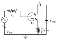
The Common Emitter (CE) configuration -- in which the emitter terminal is shared between the input loop (base-emitter) and the output loop (collector-emitter), Fig. 16.21 -- is studied in more detail than the other two configurations because it delivers the highest current gain AND the highest power gain of all three possible transistor arrangements. This happens because its INPUT is taken from a forward-biased p-n junction (the emitter-base junction), which has naturally LOW impedance, while its OUTPUT is taken from a reverse-biased p-n junction (the collector-base junction), which has naturally HIGH impedance -- and it is precisely this large mismatch between a low input impedance and a high output impedance that produces such large overall gain.\n\nSince current must be conserved at the base node, the three transistor currents obey . Two current-gain ratios are defined from these currents. The (common-emitter) DC CURRENT AMPLIFICATION FACTOR is -- for most general-purpose transistors, typically lies between about 20 and 200; a transistor with , for instance, means that for every 100 electrons flowing in the emitter-collector circuit, only 1 electron's worth of current flows out through the base -- illustrating how a SMALL change in base current can control a MUCH LARGER change in collector current, which is the essence of transistor amplification. The (common-base) ratio is . Combining these with gives , and eliminating or between the two definitions gives the standard relations linking them: and -- so knowing either ratio for a given transistor immediately gives the other. Since is always much smaller than or , is always a fairly large number while is always a fraction just under 1, and the two describe exactly the same underlying transistor action, just referenced t …
Drawn by us to help you understand the concept clearly, and verified to make sure it's accurate. For exams, practice from your textbook's own diagram.
What this figure shows. A transistor (as in Fig. 16.20a) shown with an input voltage source superimposed on a base-emitter bias applied between base and emitter, and an output taken between collector and emitter, labelled on the transistor's terminals and at the output port, with the load resistor in the collector branch (through which the collector current flows) and the base current and emitter current also marked at their respective terminals -- establishing the full set of currents/voltages (, , , , ) that the next section's char …
Drawn by us to help you understand the concept clearly, and verified to make sure it's accurate. For exams, practice from your textbook's own diagram.
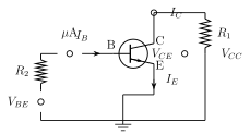
What this figure shows. A practical measurement circuit for a CE transistor: a base bias battery/supply in series with a variable resistor and a microammeter (to set and read ) connected between base and emitter; a separate collector bias battery/supply in series with the load and a milliammeter (to read ) connected between collector and emitter; and a voltmeter connected across base-emitter (to read ) and another voltmeter across collector-emitter (to read ) -- the standard two-supply, two-meter-pair layout used to trace out both the input ( vs ) and output ( vs ) char …