Physics · Ch 16 — Semiconductor Devices
Transistor as an Amplifier
Transistor as an Amplifier
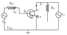
An AMPLIFIER is a device that increases the amplitude of an alternating signal -- voltage, current, or power. A transistor achieves this in the common emitter configuration by superimposing a small sinusoidal AC input signal on top of the transistor's steady DC bias (Fig. 16.25): the resulting small sinusoidal variations in base current produce correspondingly larger sinusoidal variations in collector current , and hence in the output voltage across the load resistor placed in the collector circuit. A coupling capacitor in the output circuit blocks the DC component of the collector voltage, passing through only its AC-varying part as the useful output.\n\nWith no AC signal applied, Kirchhoff's voltage law gives, for the output (collector) loop, --- (16.9), and for the input (base) loop, --- (16.10). When the AC signal IS applied, it produces a small change in the base-emitter voltage and hence in the emitter (and collector) current; from Eq. (16.9), since is fixed, any change in collector current must be balanced by an equal and opposite change in : , i.e. . This changing IS the amplified output signal, , where the AC current gain is defined as (numerically almost identical to for normal operating voltages). The VOLTAGE GAIN of the amplifier is then ; the negative sign shows the output signal is exactly OUT OF PHASE (180) with the input, and the magnitude of is what is normally quoted, . Combining current gain and voltage gain gives the POWER GAIN, . A transistor genuinely amplifies POWER (since an …
Drawn by us to help you understand the concept clearly, and verified to make sure it's accurate. For exams, practice from your textbook's own diagram.
What this figure shows. An n-p-n transistor in CE configuration with its base biased by a DC source through a base resistor , and its collector connected through the load resistor to a DC supply , emitter grounded/common to both loops. The small sinusoidal AC input signal is shown coupled IN SERIES with the base bias (superimposed on , injected into the base-emitter loop), so the actual base-emitter voltage at any instant is the DC bias plus this small AC wiggle. On the output side, a coupling CAPACITOR is drawn in series between the collector node and the output terminal, whose purpose is explicitly to BLOCK the DC component of the collector voltage from reaching the output, passing through only the AC-varying …