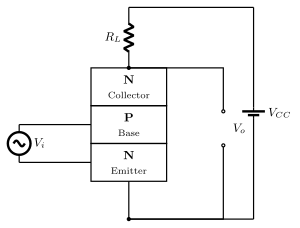
Q.(a) Describe briefly the functions of the three segments of n-p-n transistor.
You're viewing a preview — the full solution, concept, methods & PYQ mapping are locked.
Start your 14-day free trial to unlock the full solution →Part (a): Emitter (heavily doped) injects electrons, thin lightly-doped base controls the flow, collector gathers them; CE output characteristics are – curves at fixed with saturation, active and cut-off regions. Part (b): A full-wave rectifier (centre-tapped transformer + two diodes) rectifies both halves of the AC input, giving pulsating DC of average and ripple frequency .
Part (a)
Functions of the three segments
An n-p-n transistor is two p-n junctions sharing a common central p-region.
- Emitter: most heavily doped so it can inject a large number of majority carriers (electrons) into the base. Its job is to supply charge carriers.
- Base: made very thin and lightly doped. Only a tiny fraction of the injected electrons recombine here (giving a small base current); the rest are swept on to the collector. The base controls the collector current.
- Collector: moderately doped, physically the largest region so it can dissipate the heat generated. It collects the carriers that diffuse across the base.
Output characteristics (CE)
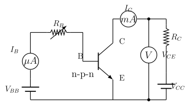
Circuit: connect a variable supply with a resistor to forward-bias the base–emitter junction, and a variable supply with to reverse-bias the collector–emitter path. The emitter terminal is common to both loops.
Method: fix the base current using ; then increase in steps using and measure the collector current each time. Repeat the whole run for several fixed values.
Result: plotting against for each gives a family of curves:
- Saturation region — for small , rises sharply.
- Active region — becomes almost independent of and ; the transistor works as an amplifier here. …
Unlock everything free for 14 days
- Full step-by-step solutions
- Concept-first explanations
- Methods, shortcuts & mistakes
- PYQ mapping + timed mock tests
Full access for 14 days. No credit card required.