Physics · Ch 16 — Semiconductor Devices
Photo Diode
Photo Diode
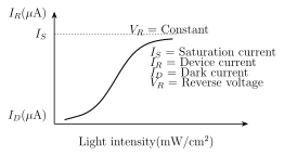
A PHOTODIODE is a special p-n junction diode designed to convert light energy directly into electrical energy -- it generates a current when exposed to light, which is why it is also called a photodetector or photosensor. Structurally (Fig. 16.9b), the junction is placed inside a glass casing so that only the junction itself is exposed to incoming light, with the rest of the device body typically painted opaque or otherwise covered. A photodiode is always operated in REVERSE bias.\n\nWorking principle: when an ordinary p-n junction is reverse biased, a small reverse saturation ('dark') current flows through it, due entirely to the MINORITY carriers present on either side of the junction (electrons are the minority carriers in the p-region, holes the minority carriers in the n-region). This dark current is essentially constant over a range of reverse bias voltages, and depends only on the concentration of minority carriers present -- not on the applied voltage itself; it is called the DARK current specifically because it flows even with no illumination at all. When the junction IS illuminated, incident photons -- provided their energy exceeds the semiconductor's band gap -- generate additional electron-hole pairs within the depletion region. The junction's own built-in electric field then separates these newly generated carriers before they can recombine: electrons are swept towards the anode side, holes towards the cathode side, adding more carriers available for conduction and thereby INCREASING the reverse current. Because this extra current depends directly on how many electron-hole pairs are generated, the photodiode's reverse current depends directly on the INTENSITY of the incident light -- and can therefore be used to measure or respond to that intensity. The total current through an illuminated photodiode is simply the sum of this light-generated photocurrent and the ever-present dark current; as illumination intensity increases, the reverse current rises (initially roughly linearly) before eventually levelling off at a SATURATION current for sufficiently strong illumination (Fig. 16.12). A photodiode's DARK RESISTANCE is defined as the ratio of the maximum reverse voltage to the dark current -- i.e. its resistance when NOT illuminated -- and the device's sensitivity can be improved by minimising this dark current.\n\nAdvantages of a photodiode include: quick response to light, a linear response (reverse current proportional to incident light intensity), high speed of operation, light weight and compact size, a wide spectral response (silicon photodiodes, for example, respond from about 190 nm in the UV up to about 1100 nm in the IR), and relatively low cost. Its main disadvantages are that its properties (like most semicon …

Drawn by us to help you understand the concept clearly, and verified to make sure it's accurate. For exams, practice from your textbook's own diagram.
What this figure shows. The standard diode symbol -- a triangle (anode) pointing to a bar (cathode) -- but with two small arrows drawn pointing INWARD towards the junction from outside the symbol (typically from the upper-left, angled towards the triangle/bar boundary), representing incident light falling on the device; the anode and cathode terminals are explicitly labelled 'Anode' and 'Cathode' respectively at the two …
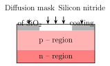
Drawn by us to help you understand the concept clearly, and verified to make sure it's accurate. For exams, practice from your textbook's own diagram.
What this figure shows. A cross-sectional structure diagram showing, from top to bottom, a thin n-type semiconductor layer at the top (the side exposed to incoming light, drawn with downward-pointing arrows striking it to represent incident photons), directly beneath it the p-n junction/depletion region, and a thicker p-type semiconductor layer below that forming the bulk of the device; metal electrical contacts are drawn on the outer faces of both the n-layer (top) and p-layer (bottom) to lead the terminals out to the a …
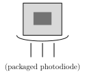
Drawn by us to help you understand the concept clearly, and verified to make sure it's accurate. For exams, practice from your textbook's own diagram.
What this figure shows. A realistic/photographic-style depiction of a small discrete photodiode component as it physically looks: a compact cylindrical or dome-topped body with a clear or lightly-tinted window at the top through which light can reach the internal junction, and two thin wire leads (one longer, marking the anode, one shorter, the cathode) protruding from the base of the package for soldering into a circuit -- illustrating that only the junction area is exposed to light while the rest of the …
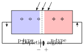
Drawn by us to help you understand the concept clearly, and verified to make sure it's accurate. For exams, practice from your textbook's own diagram.
What this figure shows. A p-n junction diode drawn in a reverse-bias circuit (battery oriented so the p-side is connected to the negative terminal and the n-side to the positive terminal, through a resistor/ammeter in series), with the p-n junction's depletion region shown between the two doped regions. Light rays (drawn as arrows or wavy lines) are shown striking the depletion region from outside, generating electron-hole pairs there (marked as +/- symbol pairs at the point of incidence); the internal electric field of the depletion region is shown sweeping the generated electrons towards the n-side and holes towards the p-side, contributing to the reverse current registered by the external meter -- illustrating the two-part current (dark current always present, plus t …
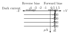
Drawn by us to help you understand the concept clearly, and verified to make sure it's accurate. For exams, practice from your textbook's own diagram.
What this figure shows. A current-vs-voltage graph for a REVERSE-biased photodiode, drawn as a family of several nearly-horizontal curves stacked one above another, each curve corresponding to a DIFFERENT (fixed) level of incident light intensity -- the topmost curve (largest reverse current magnitude) corresponds to the HIGHEST illumination level, and the curves stack downward towards a curve of minimal current (the 'dark current' curve, with essentially no light) at the bottom. Within each individual curve, the reverse current stays nearly constant/flat over a range of reverse voltages (i.e. is largely voltage-independent for a given illumination), visually demonstrating that it is the LIGHT INTENSITY, not the applied reverse voltage, that pri …
Drawn by us to help you understand the concept clearly, and verified to make sure it's accurate. For exams, practice from your textbook's own diagram.
What this figure shows. A graph with the reverse current of the photodiode on the vertical axis and the intensity of incident illumination on the horizontal axis. The curve starts near the origin (a small non-zero 'dark current' value even at zero illumination) and RISES as illumination intensity increases -- initially the rise is roughly proportional/linear -- but the curve's slope gradually flattens out at higher illumination levels, the reverse current approaching (or levelling off towards) a constant SATURATION current value at sufficiently high light intensity, rather than continuing to …