Physics · Ch 16 — Semiconductor Devices
Solar Cell or Photovoltaic Cell
Solar Cell or Photovoltaic Cell
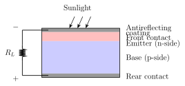
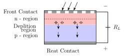
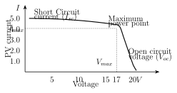
Solar energy can be harnessed in two broad ways: PHOTOTHERMAL devices, which convert solar energy into heat (mostly used for heating water), and PHOTOVOLTAIC devices, which convert solar energy directly into electrical energy using SOLAR CELLS (also called photovoltaic cells). Light incident on a solar cell produces both a current and a voltage, so it acts directly as a source of DC power -- useful anywhere from remote terrestrial locations to satellites and space stations.\n\nStructure (Fig. 16.13a): a solar cell is essentially a large-area p-n junction. Its n-side is THIN and faces the incident solar radiation directly, coated with an antireflection layer that also serves as the electrical FRONT CONTACT -- this coating lets visible light through while reflecting away IR (heat) radiation, protecting the cell's electronic properties from temperature-related degradation. The p-side is relatively THICK and forms the back of the cell, coated with a conducting BACK (or rear) contact. Making the n-side thin ensures incident light penetrates through to the depletion region, where electron-hole pair generation is most useful. A good solar-cell material must be photosensitive (able to absorb light and raise electrons to a higher energy state) and must allow those higher-energy electrons to be extracted into an external circuit, where they dissipate their energy usefully before returning to the cell.\n\nWorking: when light strikes the cell, (1) electron-hole pairs are photo-generated within the depletion region; (2) the junction's built-in electric field SEPARATES these carriers before they can recombine -- Fig. 16.13(b) -- sweeping electrons into the n-region (where they become majority carriers) and holes into the p-region (where they become majority carriers); (3) these separated charges accumulate on the p- and n-sides, building up a voltage across the cell; and (4) when an external circuit/load is connected, this accumulated charge drives a current -- called the light-generated or photo-generated current -- through it, dissipating usable power in the load. Crucially, this separation only works because the carriers are kept spatially apart by the depletion region's field; without that separation, the photo-generated electrons and holes would simply recombine and no net current or power would result.\n\nThe V-I characteristic (Fig. 16.14) is conventionally drawn in the fourth quadrant, since the cell SUPPLIES current to a load. Its intersection with the current axis gives the SHORT-CIRCUIT current (maximum current, delivered when the load is shorted, so power delivered is zero); its intersection with the voltage axis gives the OPEN-CIRCUIT voltage (maximum voltage, when no current flows, so power delivered is again zero); and somewhere between these two extremes lies the point of MAXIMUM POWER delivered to the load. Criteria for choosing a solar-cell material include: a band gap between about 1.0 and 1.8 eV, high optical absorption, good electrical conductivity, and ready availability. Most practical solar-cell materials cluster around a 1.5 eV band gap -- silicon (Eg = 1.1 eV), GaAs (Eg = 1.43 …
Drawn by us to help you understand the concept clearly, and verified to make sure it's accurate. For exams, practice from your textbook's own diagram.
What this figure shows. A cross-sectional structure diagram: a thin n-type semiconductor layer at the TOP, oriented facing upward/outward towards incoming sunlight (shown as downward arrows striking the top surface), coated on its outer (top) face with a thin antireflection coating that also serves as the electrical FRONT CONTACT (allowing visible light through while reflecting/blocking IR heat radiation). Below the n-layer lies the p-n junction/depletion region, and beneath that a much THICKER p-type semiconductor layer forming the bulk/back of the device, with a solid conducting BACK CONTACT (or rear contact) coating its bottom outer face. The overall structure is thus, top to bottom: front contact/antireflect …
Drawn by us to help you understand the concept clearly, and verified to make sure it's accurate. For exams, practice from your textbook's own diagram.
What this figure shows. A close-up of the p-n junction/depletion region of the solar cell, showing an electron-hole pair freshly generated by an absorbed photon within (or near) the depletion region -- marked as a '-' (electron) and '+' (hole) symbol pair at the point of generation, typically drawn on the p-side near the junction. Arrows are drawn showing the internal electric field of the depletion region sweeping the electron ACROSS the junction into the n-region (where it becomes a majority carrier), and correspondingly the hole moving into (or remaining in, if already generated there) the p-region (where it becomes a majority carrier) -- visually illustrating that it is this field-driven spatial separation, preventing the pair from simply recombining, that builds up …
Drawn by us to help you understand the concept clearly, and verified to make sure it's accurate. For exams, practice from your textbook's own diagram.
What this figure shows. A current-vs-voltage graph drawn in the FOURTH quadrant (i.e. the curve lies in the region where the cell is treated as SUPPLYING current to an external load, conventionally plotted with current values below the horizontal axis / voltage values still positive, reflecting the cell acting as a source rather than a sink). The curve starts at the point where it crosses the (current) axis at V = 0 -- this crossing point is labelled , the SHORT-CIRCUIT current, the maximum current the cell delivers when its terminals are shorted together. As V increases from 0, the curve stays close to this same current level for a while, then bends downward (current magnitude decreasing) and eventually crosses the (voltage) axis at I = 0 -- this crossing point is labelled , the OPEN-CIRCUIT voltage, the maximum voltage the cell can produce when no current is drawn at all. A specific point on the curve, somewhere along this bend between the two extremes, is marked as the point of MAXIMUM POWER delivered to the load, -type p …