Physics · Ch 16 — Semiconductor Devices
Zener Diode
Zener Diode
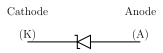
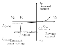
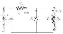
This section studies several special-purpose junction diodes: the Zener diode, the photo diode, the solar cell, and the light-emitting diode (LED). Unlike the Zener diode -- which works on the principle of controlled JUNCTION BREAKDOWN -- the other three exploit photosensitivity, a very different and equally useful property of semiconductor junctions.\n\nJunction breakdown: in Class XI we saw that if the reverse bias voltage across an ordinary p-n junction diode is increased beyond a critical value (the reverse breakdown voltage), the reverse current suddenly jumps to a large value -- and an ordinary diode is normally DAMAGED when this happens. Electrical breakdown, in general, can occur by one of two mechanisms: AVALANCHE breakdown or ZENER breakdown. Zener breakdown occurs when the reverse voltage across the junction becomes large enough that the resulting strong electric field at the junction directly pulls electrons out of the covalent bonds holding the semiconductor lattice together (rather than relying on carrier multiplication by collision, as in avalanche breakdown); these newly freed electrons become available for conduction, and as the applied reverse voltage increases further, progressively more bonds are broken and the current increases rapidly. Crucially, Zener breakdown occurs specifically in HEAVILY DOPED diodes, whose depletion layer is correspondingly narrow -- and, unlike an ordinary diode's uncontrolled breakdown, Zener breakdown does NOT damage the diode, because the diode is specifically designed (via its heavy doping) to operate safely and repeatably in this regime.\n\nA ZENER DIODE is exactly such a p-n junction diode, purpose-built to work in its own reverse breakdown region without damage, and used as a voltage regulator or voltage stabiliser (its circuit symbol has a distinctive bent/Z-shaped cathode bar, Fig. 16.7a). Its I-V characteristic (Fig. 16.7b) behaves like an ordinary diode when forward biased, but shows a sharp breakdown when reverse biased, at a voltage called the ZENER VOLTAGE : beyond , current increases suddenly and substantially while the voltage across the diode stays essentially PINNED at . itself depends on the amount of doping -- heavier doping gives a thinner depletion layer and hence a LOWER breakdown voltage, while lighter doping gives a higher one. Diodes with below about 6 V operate mainly through the true Zener mechanism; those above 6 V operate mainly through avalanche breakdown instead, but both types are still conventionally called 'Zener diodes'. A Zener diode's datasheet typically specifies: its V-I characteristic; the Zener voltage (the reverse voltage at which it is designed to operate); the maximum Zener current (or ) it can safely carry at ; its power rating (the maximum power it can dissipate); and its Zener (or dynamic) resistance (also called Zener impedance ), which is the reason the voltage across a real Zener diode is not PERFECTLY constant -- behaves like a small resistance in series with the ideal Zener, so changes in do cause small corresponding changes in .\n\nUsed as a VOLTAGE REGULATOR (Fig. 16.8), a Zener diode of breakdown voltage is connected in REVERSE bias across an input source (with ), with a series resistor limiting the current through it, and the load resistor connected in PARALLEL with the Zener diode, so the voltage across always equals . If the input voltage increases, the current through and the Zener both increase, but this extra current increase drops entirely across -- the voltage across the Zener (and hence across ) stays fixed at , since a Zener in breakdown holds its voltage constant across a wide current range. If instead stays fixed but decreases (so the load draws more current), that extra load current is simply diverted away from the Zener branch (the Zener current decreases correspondingly), again keeping unchanged. In the extr …
Drawn by us to help you understand the concept clearly, and verified to make sure it's accurate. For exams, practice from your textbook's own diagram.
What this figure shows. The standard two-terminal diode symbol -- a solid triangle (anode side) pointing towards a straight bar (cathode side) -- but with the cathode's straight bar modified into a distinctive bent or Z/S-shaped line (the two ends of the bar angled off in opposite directions, like a small 'z'), which is the feature that visually distinguishes a Zener diode's circuit symbol from an ordinary rectifier diode's plain …
Drawn by us to help you understand the concept clearly, and verified to make sure it's accurate. For exams, practice from your textbook's own diagram.
What this figure shows. A current-vs-voltage graph with current I on the vertical axis and voltage V on the horizontal axis, both axes extending into positive (forward, upper-right quadrant) and negative (reverse, lower-left quadrant) values. In the FORWARD (right) region, the curve behaves exactly like an ordinary diode: negligible current until a small forward knee voltage is crossed, after which current rises steeply. In the REVERSE (left) region, the curve first shows only a very small, flat, near-zero leakage current as reverse voltage magnitude increases -- until the voltage magnitude reaches the Zener voltage , at which point the curve turns sharply DOWNWARD (i.e. reverse current magnitude increases very rapidly) while remaining essentially PINNED at the same voltage value on the horizontal axis, i.e. a nearly vertical drop in the graph at , illustrating th …
Drawn by us to help you understand the concept clearly, and verified to make sure it's accurate. For exams, practice from your textbook's own diagram.
What this figure shows. An input DC voltage source (with ) is connected in series with a resistor ; from the junction between and the rest of the circuit, the Zener diode is connected in REVERSE bias (cathode towards the positive rail) down to the common/ground return line, and the load resistor is connected in PARALLEL with the Zener diode (i.e. and the Zener diode both sit between the same two output nodes). So the current path is: (+) -- -- output node -- splits between the Zener diode (to ground) and (to ground) -- back to (-). The voltage across is thus always equal to the voltage across the Zener diode, which stays pinned at regardless of variations in or in the load curr …
Worked out. A 5.0 V stabilised power supply must be designed from a 12 V DC input source, using a Zener diode of maximum power rating W in the Fig. 16.8 regulator circuit. (a) The maximum Zener current is found from , giving A = 400 mA. (b) The minimum series resistance follows from the voltage dropped across at this maximum current: (the source text's printed division by '400' rather than 0.4 is a units slip; using amperes consistently throughout gives the correct ). (c) With a 1 k load connected across the Zener, the load current is A = 5.0 mA. (d) At full load, the current through (fixed by and the voltage across it, essentially unchanged) splits between the Zener and the load, so the Zener current reduces to mA -- illustrating exactly how a Zener regulator self-adjusts: as load current is drawn, th …