Question 77 of 88
Q.Draw the circuit diagram of a full wave rectifier.
Puducherry TnboardTamil Nadu HSC (DGE) Board 2023Subjective· 2mImportance★★★★★
88% · 77/88 Questions
You're viewing a preview — the full solution, concept, methods & PYQ mapping are locked.
Start your 14-day free trial to unlock the full solution →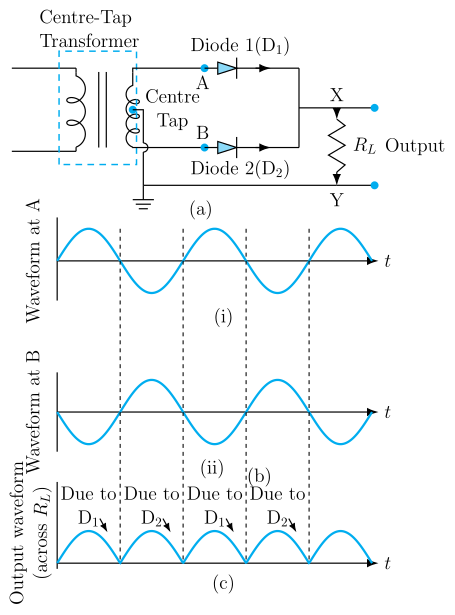
A full-wave rectifier converts the complete AC cycle (not just alternate half-cycles) to a pulsating DC output, most simply using a centre-tapped transformer with two diodes.
1. Circuit description (centre-tap type).
- The secondary winding of a step-down transformer is centre-tapped; the centre tap is taken as the common/ground reference.
- The two ends of the secondary, and , are each connected through one diode ( from , from ) to a common output terminal.
- A load resistor is connected between this common output terminal and the centre tap .
Schematically:
      A ---D1---+
Transformer       +--- output (+)
  secondary       |
      O ----------+--- R_L --- back to O (ground/-)
      B ---D2---+
2. Working.
- During the half-cycle when is at a higher potential than , diode is forward biased and conducts, sending current through from top to bottom; is reverse biased and does not conduct.
- During the next half-cycle, becomes positive with respect to ; now conducts and is cut off, but current again flows through in the same direction as before. …
Unlock everything free for 14 days
- Full step-by-step solutions
- Concept-first explanations
- Methods, shortcuts & mistakes
- PYQ mapping + timed mock tests
Full access for 14 days. No credit card required.