Physics · Ch 16 — Semiconductor Devices
NOR Gate
NOR Gate
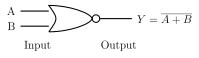
The NOR gate is formed by connecting the output of an OR gate into the input of a NOT gate -- i.e. it is simply an OR gate followed by inversion -- and its output is therefore the exact OPPOSITE of a plain OR gate's, for every input combination: the output Y is HIGH (1) only when BOTH inputs A and B are simultaneously LOW (0); for every other combination, the output is LOW (0). Its Boolean expression is (Fig. 16.31), the symbol being an ordinary OR-gate shape with a small inversion bubble added at its output. Like NAND, NOR is also a UNIVERSAL GATE: any other logic gate or digital fun …
Drawn by us to help you understand the concept clearly, and verified to make sure it's accurate. For exams, practice from your textbook's own diagram.
What this figure shows. The identical curved-back, pointed-front OR-gate body shape as Fig. 16.28, with the same two input lines A and B entering the concave back edge -- but with a small open CIRCLE ('bubble') added at the output tip, exactly like the NOT gate's inversion bubble, marking that this gate's output is the logical negation of the plain OR gate's; the output line (labelled $Y=\overline{A+B} …
Input A | Input B | Output Y
0 | 0 | 1
0 | 1 | 0 …