Electronics · Ch 5 — Operational Amplifiers
Applications of op-amp with negative feedback
Applications of op-amp with negative feedback
The applications of an op-amp are broadly classified as linear and non-linear:
- Linear applications — the output is directly proportional to the input. Examples: the inverting amplifier and the non-inverting amplifier.
- Non-linear applications — the output is not directly proportional to the input. Examples: the integrator, the differentiator and the logarithmic amplifier.
Why feedback is needed. An op-amp has a very high open loop gain, so on its own it can amplify only very small signals without distortion. For any larger signal the output tries to exceed the supply voltages and , and clipping occurs. To make the device usable, negative feedback is applied — a portion of the output is fed back to the input, either directly or through a resistor network. With feedback the op-amp becomes a very versatile device usable over a wide range of AC and DC applications, and its overall gain is set by the external resistors rather than by the huge, variable open loop gain.
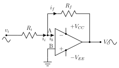
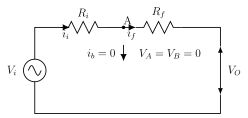
Virtual ground (virtual short) concept. Consider an ideal op-amp with negative feedback (Figures 5.4.1 and 5.4.2). Let be the voltage at the inverting terminal, the voltage at the non-inverting terminal, the current into the op-amp, and , the input and feedback resistors. For an ideal op-amp the open loop gain and the input impedance . Since
So the two input terminals always sit at the same voltage (a virtual short). If is grounded then : the inverting terminal is at zero volts even though it is not physically connected to ground — this is the virtual ground. And because , no current enters the op-amp, i.e. . Note the virtual ground holds for voltage only, not for current flow. This single idea makes every feedback derivation below straightforward.
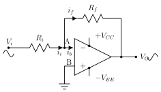
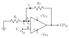
Inverting amplifier. An inverting amplifier gives an output that is 180° out of phase with the input. The input is applied to the inverting terminal through , the non-inverting terminal is grounded, and is the feedback resistor from output to the inverting node A (Figure 5.4.3). With the virtual ground and , applying KCL at node A gives :
Putting : , so
The minus sign shows the 180° phase inversion.
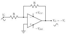
Inverter (sign changer). The inverter is a special case of the inverting amplifier that produces an output equal in magnitude but opposite in phase to the input. It is obtained by making (Figure 5.4.4, both resistors labelled R), which gives
The output is simply the inversion of the input, and the circuit is called an op-amp inverter.
Non-inverting amplifier. A non-inverting amplifier gives an output in phase with the input. The input is applied to the non-inverting terminal, the inverting terminal is grounded through , and is the feedback resistor (Figure 5.4.5). Now and . Applying KCL at node A ():
Putting and solving:
The gain is always greater than one and the output is in phase with the input. …
In an ideal op-amp with negative feedback, the infinite open loop gain forces the two input terminals to the same voltage, . When the non-inverting terminal is grounded, the inverting terminal sits at 0 V without being physically grounded — a virtual ground. Infinite input impedance also makes the current into the op-a …
Drawn by us to help you understand the concept clearly, and verified to make sure it's accurate. For exams, practice from your textbook's own diagram.
Reproduces textbook Figure 5.4.1 (Virtual Ground concept). Input reaches inverting node A through input resistor (input current ); feedback resistor carries from output back to node A; is the current into the op-amp; the non-inverting terminal B is grounded; supplies , ; output $V_O …
Drawn by us to help you understand the concept clearly, and verified to make sure it's accurate. For exams, practice from your textbook's own diagram.
Reproduces textbook Figure 5.4.2 (Equivalent circuit to show Virtual Ground concept). Source drives resistor (current ) into node A, from which (current ) continues to the output ; the annotations and $i_b = …
Drawn by us to help you understand the concept clearly, and verified to make sure it's accurate. For exams, practice from your textbook's own diagram.
Reproduces textbook Figure 5.4.3 (Inverting Amplifier). Input enters inverting node A through ; feeds back from output to node A; non-inverting terminal B is grounded; supplies , ; output is the inverted sine, 180° out of phase with the inpu …
Drawn by us to help you understand the concept clearly, and verified to make sure it's accurate. For exams, practice from your textbook's own diagram.
Reproduces textbook Figure 5.4.4 (Inverter). Same as the inverting amplifier but both resistors are equal (labelled R, i.e. ); the non-inverting terminal is grounded; supplies , ; output labelled $V_O = - …
Drawn by us to help you understand the concept clearly, and verified to make sure it's accurate. For exams, practice from your textbook's own diagram.
Reproduces textbook Figure 5.4.5 (Non-inverting amplifier). Input is applied to the non-inverting terminal B; the inverting terminal (node A) is grounded through ; feeds back from output to node A carrying ; supplies , ; output is in phase with the inpu …
Drawn by us to help you understand the concept clearly, and verified to make sure it's accurate. For exams, practice from your textbook's own diagram.
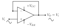
Reproduces textbook Figure 5.4.6 (Buffer amplifier). The output is shorted directly back to the inverting terminal (feedback resistor removed); input is applied to the non-inverting terminal; supplies , ; output labelled , in phase, unity …
and . The negative sign indicates the 180° phase inversion between output and input. is the input applied through to the inverting terminal, the feedback resistor and the output; the gain is set purely by the …
When the inverting amplifier becomes an inverter: . The output equals the input in magnitude but is opposite in phase. This unity-gain special case is used purely as a sign changer, giving a 180° phase shift with no amplification; and are the equal feedback and input resis …
and . The gain is always greater than one and the output is in phase with the input. Here is applied to the non-inverting terminal, is grounded through the inverting node and is the feedback resistor; the resistor rati …
With in the non-inverting result, and . Unity gain, no phase shift, high input impedance and low output impedance make it an idea …