Electronics · Ch 5 — Operational Amplifiers
Digital to analog converter (DAC)
Digital to analog converter (DAC)
A Digital-to-Analog Converter (DAC) converts a digital input (binary, BCD or another digital code) into an analog output — usually a DC voltage — whose value is proportional to the binary number applied. Two common methods are the R-2R ladder network DAC and the binary weighted resistance DAC.
4-bit R-2R ladder network DAC
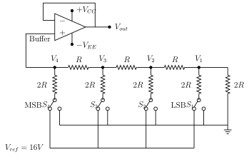
Figure 5.9.1 shows a 4-input DAC built from a ladder using only two resistor values, and (for example 1 kΩ and 2 kΩ). Each binary input is a switch that connects either to (logic 1) or to 0 V (logic 0). The ladder output is buffered by an op-amp voltage follower to give .
When all switches are at 0 V, . Taking one switch to 16 V at a time gives:
- input :
- input :
- input :
- input :
By superposition, several logic-1 inputs simply add their individual contributions, so the analog output is proportional to the binary number. Table 5.9.1 lists for all sixteen 4-bit inputs.
Binary weighted resistance DAC
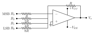
Here weighted resistors , , and feed a summing (inverting) amplifier (figure 5.9.2). A logic 0 corresponds to 0 V and a logic 1 to 5 V. The most significant bit (MSB) enters through and the least significant bit (LSB) through , with a feedback resistor . For a single LSB input , ; for the MSB alone , . The output is therefore proportional to the digital input. Table 5.9.2 gives the full output chart.
Analog-to-Digital Converter (ADC)
An ADC performs the reverse operation, converting an analog input into a digital output that can be displayed. For example, a temperature difference sensed by a thermocouple appears as an analog voltage, which an ADC turns into digital form.
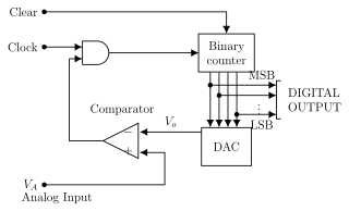
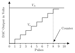
The counting ADC (figure 5.9.3) uses a comparator, a binary counter, a DAC and an AND gate. A clear pulse first resets the counter to zero. The clock then advances the counter; its binary output drives a DAC whose output is a rising staircase waveform (figure 5.9.4). The comparator continuously compares this staircase with the analog input . While , the comparator output is high, keeping the AND gate open so clock pulses reach the counter. Once exceeds , the comparator output goes low, the AND gate closes, and the counter stops when . The value held in the counter is the digital equivalent of the analog input.
Open-loop applications of the op-amp: comparator and Schmitt trigger
All the circuits above use negative feedback. When the op-amp is used without negative feedback it works in an open-loop configuration, comparing one input against the other.
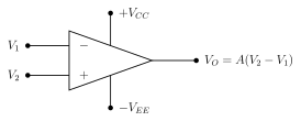
Working of a comparator. In the basic comparator (figure 5.9.5) the output is , the product of the very large open-loop gain (of the order of or more) and the input difference. Even a few millivolts of difference drives the output into saturation at or :
- if , then
- if , then
With a fixed reference on one terminal and a varying signal on the other, the comparator gives a two-state (digital) output that switches between and .
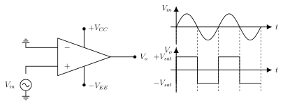
Zero crossing detector. A zero crossing detector (figure 5.9.6) applies the varying signal to the non-inverting terminal with the inverting terminal grounded. Then when and when . The output switches state at every zero crossing of the input, converting a sine wave into a square wave. …
Drawn by us to help you understand the concept clearly, and verified to make sure it's accurate. For exams, practice from your textbook's own diagram.
Figure 5.9.1 shows the 4-bit R-2R ladder DAC. A horizontal chain of series resistors R links the ladder nodes V4-V3-V2-V1, and from each node a 2R resistor drops to a switch (S4 = MSB, S3, S2, S1 = LSB) that selects either the Vref = 16V rail or ground; a 2R terminating resistor closes the ladder. The ladder top node drives an op-amp voltage follower (labelled Buffer, +Vcc/-Vee) whose output is Vout. The …
Table 5.9.1 — DAC output for a 4-bit binary input (Vref = 16 V):
| Binary input | Vout (in volts) |
|---|---|
| 0000 | 0 |
| 0001 | 1 |
| 0010 | 2 |
| 0011 | 3 |
| 0100 | 4 |
| 0101 | 5 |
| 0110 | 6 |
| 0111 | 7 |
| 1000 | 8 |
| 1001 | 9 |
| 1010 | 10 |
| 1011 | 11 |
Drawn by us to help you understand the concept clearly, and verified to make sure it's accurate. For exams, practice from your textbook's own diagram.
Figure 5.9.2 shows the 4-bit binary weighted resistance DAC. Four digital inputs each pass through a weighted resistor to the inverting (summing) input of the op-amp: MSB B3 through R, B2 through 2R, B1 through 4R, LSB B0 through 8R. The non-inverting input is grounded, the feedback resistor is R, supply pins +Vcc/-Vee, output Vo. Logic 0 = 0 V and logic 1 = …
Table 5.9.2 — DAC output for the binary weighted resistance network (each bit is 0 V or 5 V):
| B3 | B2 | B1 | B0 | Vout (in volts) |
|---|---|---|---|---|
| 0 | 0 | 0 | 0 | 0.000 |
| 0 | 0 | 0 | 5 | -0.625 |
| 0 | 0 | 5 | 0 | -1.250 |
| 0 | 0 | 5 | 5 | -1.875 |
| 0 | 5 | 0 | 0 | -2.500 |
| 0 | 5 | 0 | 5 | -3.125 |
| 0 | 5 | 5 | 0 | -3.750 |
| 0 | 5 | 5 | 5 | -4.375 |
| 5 | 0 | 0 | 0 | -5.000 |
| 5 | 0 | 0 | 5 | -5.625 |
| 5 | 0 | 5 | 0 | -6.250 |
| 5 | 0 | 5 | 5 | -6.875 |
Drawn by us to help you understand the concept clearly, and verified to make sure it's accurate. For exams, practice from your textbook's own diagram.
Figure 5.9.3 shows the counting ADC block diagram. Clear and Clock lines enter on the left; the Clock feeds an AND gate whose output drives a Binary counter (Clear resets it). The counter's binary output bus (MSB to LSB) is the digital output and also feeds a DAC; the DAC output Vo goes to one input of a comparator, whose other input is the analog input VA. The comparator output …
Drawn by us to help you understand the concept clearly, and verified to make sure it's accurate. For exams, practice from your textbook's own diagram.
Figure 5.9.4 shows the DAC staircase waveform of the counting ADC. The vertical axis is DAC output in volts and the horizontal axis is clock pulses (0 to 10). The output Vo climbs in equal steps with each pulse; a horizontal line marks the analog input level VA, and a vertical dotted line shows where the staircase rea …
Drawn by us to help you understand the concept clearly, and verified to make sure it's accurate. For exams, practice from your textbook's own diagram.
Figure 5.9.5 shows the basic comparator. The op-amp symbol has input V1 on the inverting (-) terminal and V2 on the non-inverting (+) terminal, with supply pins +Vcc (top) and -Vee (bottom). The output is Vo = A(V2 - V1). This exact terminal assignment (V1 on -, V2 on +) matches the printed …
, where is the open-loop gain (order or more). The output saturates: if then ; if th …
Drawn by us to help you understand the concept clearly, and verified to make sure it's accurate. For exams, practice from your textbook's own diagram.
Figure 5.9.6 shows the zero crossing detector. LEFT: the op-amp has the varying source Vin on the non-inverting (+) input and the inverting (-) input grounded, supply pins +Vcc/-Vee, output Vo. RIGHT: the input Vin is a sine wave and the output Vo is a square wave between +Vsat and -Vsat, with transition …
Drawn by us to help you understand the concept clearly, and verified to make sure it's accurate. For exams, practice from your textbook's own diagram.
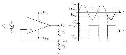
Figure 5.9.7 shows the Schmitt trigger. LEFT: the varying source Vin drives the inverting (-) input; the output feeds a resistor divider R1 (top) and R2 (to ground), and the R1-R2 junction Vref is fed back to the non-inverting (+) input (positive feedback). Supply pins +Vcc (top) and -Vee (bottom). RIGHT: the sine input Vin is shown with dashed reference lines at +Vref and -Vref, and the output Vo is a square wave between +Vsat and -Vsat that switches when Vin crosses +Vref/-Vref. Note for the redraw: show only the -Vee supply pin at the op-amp's bottom; a stray '-Vee' label printed near …
, so . The output is when and when ; the shifting trip level gives noise imm …