Electronics · Ch 5 — Operational Amplifiers
Differential amplifier
Differential amplifier
The differential amplifier — also called the difference amplifier or emitter-coupled amplifier — is the main building block of IC amplifiers and is the basic input stage of an integrated op-amp. It is a direct-coupled amplifier that, as its name implies, amplifies the difference between its two input signals.
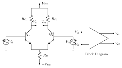
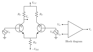
Basic circuit. The basic differential amplifier (Figure 5.2.1) uses two identical transistors and , two collector resistors and , and a common emitter resistor . The two input signals and are applied to the bases of the two transistors, and the two outputs and are taken from the collectors. Two power supplies and bias the circuit.
Four modes. Depending on how many inputs are driven and how many outputs are taken, a differential amplifier can be operated in four modes:
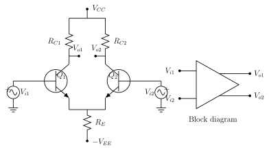
- Double-ended input and double-ended output (dual input, balanced output) — Figure 5.2.2a.
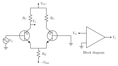
- Single-ended input and single-ended output (single input, balanced output) — Figure 5.2.2b.
- Double-ended input and single output (dual input, unbalanced output) — Figure 5.2.2d.
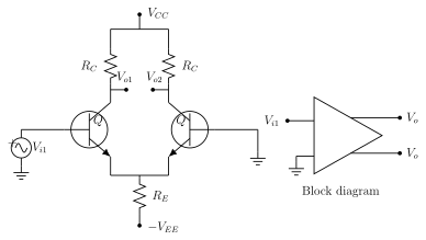
- Single-ended input and double-ended output (single input, balanced output) — Figure 5.2.2c.
The parenthetical descriptions for the four modes are reproduced exactly as printed in the textbook. The figure captions themselves give the clearest names: 5.2.2a dual input, balanced output; 5.2.2b single input, unbalanced output; 5.2.2c single input, balanced output; 5.2.2d dual input, unbalanced output.
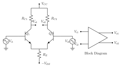
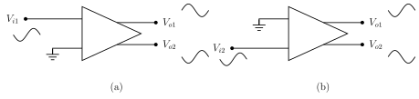
Working of the dual-input balanced-output amplifier. The operation is analysed using the superposition theorem by taking one input at a time (Figure 5.2.3, phases shown in Figure 5.2.4):
- Condition 1 — apply , ground : is the base input of and its output is taken at the collector, so works as a common-emitter (CE) amplifier and is out of phase with . At the same time appears at the emitter of , so works as a common-base (CB) amplifier whose collector output is in phase with .
- Condition 2 — apply , ground : now acts as a CE amplifier and is out of phase with ; acts as a CB amplifier, and reaching its emitter appears amplified and in phase at the collector as .
When both inputs are applied together, the output is measured between the two collectors, and the voltage gain is
(The textbook writes the difference of the two inputs using a tilde, ; it simply means the difference between the two input voltages.)
Common-mode operation. When the same (common) input is applied to both terminals, the amplifier is in common-mode operation. A good differential amplifier refuses to amplify common-mode signals: the equal inputs drive both identical transistors equally, and the resulting output contributions are opposite in polarity and cancel. By superposition, if then and , so for a dual-input single-output amplifier , i.e. the common-mode gain is ideally zero. The common-mode gain is
Differential-mode operation. When two opposite-polarity signals are applied to the two inputs, the amplifier is in differential mode: the difference of the two signals is amplified and appears at the output. The gain for this input is the differential-mode voltage gain . By superposition, if then and , and
where is the AC emitter resistance of the transistors. …
A direct-coupled difference (emitter-coupled) amplifier that amplifies the difference between its two input signals. Built from two identical transistors with a shared emitter resistor, it is the main building block of IC amplifier …
Drawn by us to help you understand the concept clearly, and verified to make sure it's accurate. For exams, practice from your textbook's own diagram.
Reproduces textbook Figure 5.2.1 (Differential Amplifier). Supply feeds collector resistors and to the collectors of NPN transistors and ; collector outputs and are taken from the two collectors. Bases are driven by inputs and ; the emitters share a common resistor to . A block-diagram triangle on the right shows two …
Drawn by us to help you understand the concept clearly, and verified to make sure it's accurate. For exams, practice from your textbook's own diagram.
Reproduces textbook Figure 5.2.2a (Dual input and balanced output differential amplifier). Both bases are driven by separate AC sources and , and outputs , are taken from both collectors. Illus …
Drawn by us to help you understand the concept clearly, and verified to make sure it's accurate. For exams, practice from your textbook's own diagram.
Reproduces textbook Figure 5.2.2b (Single input and unbalanced output differential amplifier). Only one base is driven by AC source ; a single output is taken from one collector while the other transistor …
Drawn by us to help you understand the concept clearly, and verified to make sure it's accurate. For exams, practice from your textbook's own diagram.
Reproduces textbook Figure 5.2.2c (Single input and balanced output differential amplifier). One base is driven by AC source ; two outputs and are taken from both collectors. Illustrates mode 4 (sin …
Drawn by us to help you understand the concept clearly, and verified to make sure it's accurate. For exams, practice from your textbook's own diagram.
Reproduces textbook Figure 5.2.2d (Dual input and unbalanced output differential Amplifier). Both bases are driven by and , but a single output is taken from one collector only. Illustrates mode 3 (dua …
Drawn by us to help you understand the concept clearly, and verified to make sure it's accurate. For exams, practice from your textbook's own diagram.
Reproduces textbook Figure 5.2.3 (Dual input balanced output Differential Amplifier). This is the circuit whose working is analysed by superposition: inputs , drive the two bases and outputs , come from the two collectors with the shared emitter resistor . It …
Drawn by us to help you understand the concept clearly, and verified to make sure it's accurate. For exams, practice from your textbook's own diagram.
Reproduces textbook Figure 5.2.4 (Working of Dual input Balanced output Differential Amplifier), shown as two sub-diagrams (a) and (b). In (a) only is applied: output is in-phase-inverted relative to (CE action) and is the opposite phase (CB action). In (b) only is applied and the roles swap. The waveforms make the ou …
— the output is measured between the two collectors when both inputs are applied. The textbook prints the input difference with a …
— the gain for a signal applied equally (in common) to both inputs; ideally driven towards zero by a large . Here is the collector resistance and the common emitter resistance; a large pushes close to zero, which is what lets the differe …
, where is the AC emitter resistance of the transistors. This is the gain seen by the difference of the two input signals. A large together with a small common-mode gain gives a high CMRR, so the stage amplifies the wanted differen …
; ideally so . Expressed in decibels, . A high CMRR means strong amplification of difference signals and strong …