Electronics · Ch 5 — Operational Amplifiers
Op-Amp as summing amplifier
Op-Amp as summing amplifier
Op-amp as a summing amplifier
An op-amp summing amplifier produces an output equal to the sum of several input voltages. Because the op-amp is operated in the inverting mode, the output appears as the negative sum of the inputs, with each input scaled by its own gain factor. It is one of the most frequently tested linear op-amp circuits in the Karnataka 2nd PUC Electronics board exam.
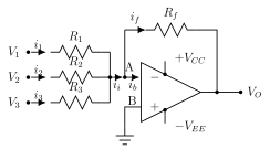
In the circuit of figure 5.5.1, three input voltages , and are applied to the inverting terminal (node A) through resistors , and . A feedback resistor connects the output back to node A, and the non-inverting terminal (node B) is grounded.
Treating the op-amp as ideal (open-loop gain , input impedance ), two facts follow: the bias current into the op-amp is zero (), and by the virtual-ground concept . Applying Kirchhoff's current law at node A, the total input current equals the feedback current, , i.e.
Putting gives the summing-amplifier output
If all resistors are equal, , this reduces to — the output is simply the negative sum of the inputs, so the circuit is also called an op-amp inverting adder. By choosing the input resistors relative to , each input can be given a different weight, which lets the same circuit realise a weighted sum such as .
Op-amp as a subtractor (difference amplifier)
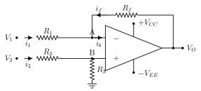
A difference amplifier, or subtractor, gives an output proportional to the difference of two input voltages. In figure 5.5.2, is applied through to the inverting terminal (node A) and through to the non-inverting terminal (node B); connects node B to ground and is the feedback resistor.
The output is found using the superposition theorem:
- With alone ( grounded) the circuit behaves as an inverting amplifier, giving . …
Drawn by us to help you understand the concept clearly, and verified to make sure it's accurate. For exams, practice from your textbook's own diagram.
Figure 5.5.1 shows the op-amp inverting adder. Inputs V1, V2 and V3 join at the inverting terminal (node A) through R1, R2 and R3 carrying currents i1, i2, i3 (summed as i_i); the feedback resistor Rf carries current i_f from the output back to node A, and the non-inverting terminal (node B) is grounded. Supply pins are +Vcc (top) and -Vee (bottom), output Vo at right. This …
; for equal resistors this reduces to , …
Drawn by us to help you understand the concept clearly, and verified to make sure it's accurate. For exams, practice from your textbook's own diagram.
Figure 5.5.2 shows the op-amp difference amplifier. V1 reaches the inverting terminal (node A) through R1 (current i1) with feedback resistor Rf; V2 reaches the non-inverting terminal (node B) through R2 (current i2), and R3 connects node B to ground. Supply pins +Vcc and -Vee, output Vo. It is anal …
; for equal resistors this becomes . enters the inverting terminal through (= ) and the non-inverting terminal through , with to ground and …