Electronics · Ch 5 — Operational Amplifiers
Operational Amplifier
Operational Amplifier
Having seen the differential amplifier at its input, we now look at the op-amp as a complete device through its AC equivalent circuit and its characteristics.
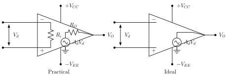
AC equivalent circuit. Figure 5.3.1 shows the op-amp modelled in both a practical and an ideal form. In the practical model a differential input voltage appears across the two input terminals, an input resistance is drawn between them, and a dependent voltage source drives the output through an output resistance ; the device is powered by and . In the ideal model there is no input-resistance branch () and no output resistance (), so the dependent source connects straight to the output.
Ideal vs practical characteristics. A practical op-amp has very high input impedance , very high voltage gain and low output impedance ; an ideal op-amp has infinite input impedance, infinite voltage gain and zero output impedance. The main characteristics are:
- Open Loop Gain — the gain of the amplifier without feedback. It is infinite for an ideal op-amp and of the order of for a practical one.
- Input Impedance — the impedance seen looking into the two input terminals. Ideally infinite, so the op-amp can be driven by any source without loading the previous stage; practically a few .
- Output Impedance — the impedance seen looking back into the output terminal. Ideally zero, so the op-amp can drive any number of devices without getting loaded; practically a few tens of .
- Bandwidth — ideally infinite, meaning the op-amp amplifies signals from zero to infinite hertz without attenuation; practically a few MHz.
- CMRR — the ability to reject common-mode signals such as noise while amplifying differential signals. Ideally infinite; a practical value is around 90 dB.
- Slew Rate — the maximum rate of change of the output voltage when a large signal is applied to the closed-loop amplifier. It shows how well the op-amp handles rapidly varying signals (its response to changes in input). For an ideal op-amp the response time is zero, so the slew rate is infinite. Its unit is V/μs and it is given by .
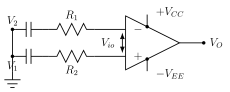
Input offset voltage. Ideally, when the two inputs are at the same voltage the output should be zero, since . In practice it is not, so a small voltage — the input offset voltage — must be applied between the two input terminals to force the output to zero. This is also called the balancing technique and is shown in Figure 5.3.2. …
Drawn by us to help you understand the concept clearly, and verified to make sure it's accurate. For exams, practice from your textbook's own diagram.
Reproduces textbook Figure 5.3.1 (AC equivalent circuit of Op-Amp). Left (Practical): a triangle with differential input across the inputs, input resistance between them and a dependent source feeding the output through output resistance ; supplies and . Right (Ideal): the same triangle but with (no branch) and , the source connecting directl …
Drawn by us to help you understand the concept clearly, and verified to make sure it's accurate. For exams, practice from your textbook's own diagram.
Reproduces textbook Figure 5.3.2 (Input offset voltage). Input reaches the inverting terminal through resistor and input reaches the non-inverting terminal through resistor ; a small offset voltage is marked between the two input terminals. Supplies and , output . Sho …
Drawn by us to help you understand the concept clearly, and verified to make sure it's accurate. For exams, practice from your textbook's own diagram.
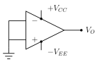
Reproduces textbook Figure 5.3.3 (Output offset voltage). Both the inverting and non-inverting terminals are tied to ground; supplies and ; the output still shows a small error voltage caused by the mismatch in of the two input t …
Drawn by us to help you understand the concept clearly, and verified to make sure it's accurate. For exams, practice from your textbook's own diagram.
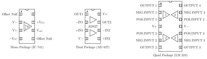
Reproduces textbook Figure 5.3.4 (Pin diagrams of mono, dual and quad ICs), redrawn from the pin-function facts only. Mono Package IC 741 (8-pin): 1 Offset Null, 2 V- (inverting), 3 V+ (non-inverting), 4 -Vcc, 5 Offset Null, 6 Vout, 7 +Vcc, 8 NC. Dual Package AD 827 (8-pin, two op-amps): 1 OUT1, 2 -IN1, 3 +IN1, 4 V-, 5 +IN2, 6 -IN2, 7 OUT2, 8 V+. Quad Package LM 324 (14-pin, four op-amps): 1 OUTPUT1, 2 NEG.INPUT1, 3 POS.INPUT1, 4 V+, 5 POS.INPUT2, 6 NEG.INPUT2, 7 OUTPUT2, 8 O …
(measured in V/μs) — the maximum rate at which the output voltage can change for a large input signal. Ideally infinite; a typical p …
| Characteristics | Ideal Op-Amp | Practical Op-Amp |
|---|---|---|
| Open loop gain | In the order of | |
| Input Impedance | Few | |
| Output Impedance | 0 | Few ohms |
| Band width | Few MHz | |
| CMRR | 90 dB |