Q.Explain briefly with the help of a circuit diagram, charges and depletion layer, how V-I characteristics of a p-n junction diode are obtained in reverse bias. Draw the shape of the curves obtained. Why is the current under reverse bias almost independent of the applied potential up to a critical voltage? OR Why should a photodiode be operated at a reverse bias? Draw the biasing circuit of an illuminated photodiode and characteristic curves.
You're viewing a preview — the full solution, concept, methods & PYQ mapping are locked.
Start your 14-day free trial to unlock the full solution →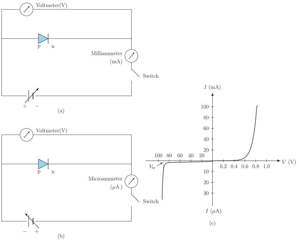
Reverse bias widens the depletion layer and raises the barrier; the tiny resulting current is carried by minority carriers and stays nearly constant until breakdown.
Circuit: The p-n junction diode is connected with the p-side to the negative terminal and the n-side to the positive terminal of a battery, in series with a microammeter (to measure the small reverse current) and a rheostat to vary the reverse voltage.
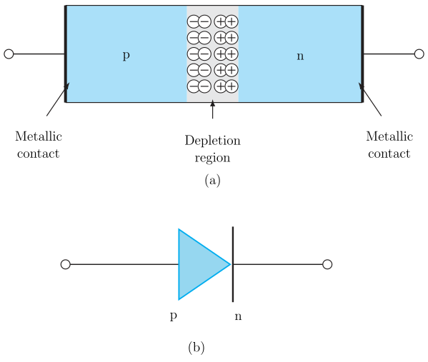
Depletion layer / charges under reverse bias: The applied reverse voltage pulls majority carriers (holes in p, electrons in n) further away from the junction, widening the depletion layer and increasing the potential barrier across it. This strongly opposes the flow of majority carriers, so almost no majority-carrier current flows.
V-I characteristic: As the reverse voltage is increased from zero, a very small current (of the order of µA) flows, and it quickly saturates — remaining almost constant as reverse voltage is increased further — until, at a certain critical (breakdown) voltage, the current rises sharply (avalanche/Zener breakdown). The reverse characteristic is thus a nearly flat curve very close to the voltage axis, followed by a sharp knee at breakdown.
…
Unlock everything free for 14 days
- Full step-by-step solutions
- Concept-first explanations
- Methods, shortcuts & mistakes
- PYQ mapping + timed mock tests
Full access for 14 days. No credit card required.