Q.(a) Differentiate between three segments of an n-p-n transistor on the basis of their size and level of doping.
You're viewing a preview — the full solution, concept, methods & PYQ mapping are locked.
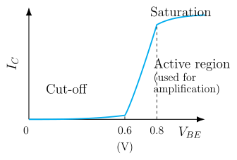
Start your 14-day free trial to unlock the full solution →A transistor has three differently doped and sized regions (emitter, base, collector). Its transfer characteristic (output current vs. input voltage) has an active region where a small change in base-emitter voltage produces a large change in collector current — this linear portion is used for amplification.
The Concept: Why a Transistor Amplifies
A transistor is not just three pieces of semiconductor stuck together. It works because of a clever asymmetry. The emitter is heavily doped to inject many charge carriers (electrons for n-p-n). The base is very thin and lightly doped so most injected carriers cross it without recombining. The collector is moderately doped and large to efficiently collect those carriers.
The magic happens in the active region of the transfer characteristic. Here, the base-emitter junction is forward-biased and the collector-base junction is reverse-biased. A tiny change in base-emitter voltage () causes an exponential change in base current (), which in turn controls a much larger collector current (). The ratio is the current gain , typically 50–200. That's amplification — a small input signal controls a large output.
Step-by-Step Solution
(a) Differentiating the Three Segments
The three regions of an n-p-n transistor differ in three key ways: size, doping concentration, and function.
| Feature | Emitter (E) | Base (B) | Collector (C) |
|---|---|---|---|
| Size | Moderate | Very thin (a few m) | Largest |
| Doping | Heaviest () | Lightest () | Moderate () |
| Role | Injects electrons | Passes electrons to collector | Collects electrons |
Why these differences matter:
- Heavy emitter doping ensures a huge supply of electrons to inject into the base. This gives high current gain.
- Thin, lightly doped base minimises recombination. Most electrons (over 95%) survive the journey across the base and reach the collector. If the base were thick or heavily doped, many electrons would recombine with holes, and the transistor would have poor gain.
- Large, moderately doped collector can handle the collected current and dissipate heat. It doesn't need heavy doping because it doesn't inject carriers — it just receives them.
A common mistake is thinking all three regions are equally doped. The emitter is always the most heavily doped region in a bipolar junction transistor. The base is the lightest.
(b) Transfer Characteristic and Amplification
The transfer characteristic of a transistor in common-emitter configuration plots the output current () against the input voltage (). It is essentially the same shape as the diode characteristic of the base-emitter junction, scaled by the current gain .
Drawing the plot:
- Axes: X-axis = (base-emitter voltage), Y-axis = (collector current).
- Shape: The curve stays essentially at zero for below about 0.6 V (silicon) — the cut-off region. It then rises steeply and almost linearly through a short 'knee' between roughly 0.6 V and 0.8 V — this rising, near-linear stretch is the active region — and finally flattens out again once the transistor enters saturation beyond about 0.8 V.
Which portion is used for amplification?
The active region — the steep, nearly linear portion between the "knee" (around 0.6 V) and the onset of saturation (around 0.8 V).
Why this region? …
Unlock everything free for 14 days
- Full step-by-step solutions
- Concept-first explanations
- Methods, shortcuts & mistakes
- PYQ mapping + timed mock tests
Full access for 14 days. No credit card required.