Intuition First: Why a Zener Diode Can "Hold" a Voltage
Imagine a pressure relief valve in a water pipe. If the water pressure gets too high, the valve opens just enough to let some water escape, keeping the pressure downstream constant — no matter how much the upstream pressure fluctuates. A Zener diode does the same thing, but with voltage.
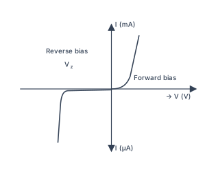
In a normal diode, reverse bias blocks current completely — until you push too hard and destroy it. A Zener diode is specially designed so that when you reverse-bias it past a certain voltage (the Zener voltage, VZ), it doesn't break — it conducts steadily without damage. And here's the magic: once it starts conducting in breakdown, the voltage across it stays almost exactly at VZ, even if the current through it changes dramatically.
That flat voltage is what makes it a regulator.
The Precise Statement
A Zener diode, when reverse-biased into its breakdown region, maintains a nearly constant voltage VZ across its terminals over a wide range of reverse currents. In a circuit, this allows it to hold a fixed output voltage despite variations in the input supply or the load current — provided the current through the Zener stays within its safe operating limits.
How It Works in a Circuit
The simplest Zener regulator looks like this:
- A series resistor Rs connects the unregulated input Vin (which is higher than VZ) to the Zener diode.
- The Zener is reverse-biased, with its cathode toward the positive supply.
- The load RL is connected across the Zener diode.
The resistor is the workhorse. It drops the excess voltage (Vin−VZ) and limits the current. The Zener does the regulation.
Case 1: Input voltage rises
If Vin increases, the current through Rs tries to increase. But the Zener is already in breakdown — it simply absorbs the extra current, and the voltage across it stays at VZ. The load sees no change.
Case 2: Load draws more current
If the load resistance decreases (more current needed), that current comes from the Zener branch. The Zener current drops by exactly the same amount. The total current through Rs stays the same, so the voltage drop across Rs doesn't change — and VZ remains constant.
The Zener acts like a variable resistor that automatically adjusts its resistance to keep the voltage fixed. When the load demands more current, the Zener "gives up" some of its own current. When the load demands less, the Zener takes the extra.
The Key Formula
IZ=RsVin−VZ−IL
Where:
- IZ is the current through the Zener diode
- IL=VZ/RL is the load current
- The first term is the total current through Rs
For regulation to work, IZ must always stay between IZ(min) (the minimum current needed to keep the Zener in breakdown) and IZ(max) (the maximum current the Zener can handle without overheating).
The Two Critical Limits
A Zener regulator fails if: …