Q.(a)
🔒You're viewing a preview — the full solution, concept, methods & PYQ mapping are locked.
🔒 Start your 14-day free trial to unlock the full solution →Part (a)Concept understanding — P-N Junction Formation
P-N Junction Formation: From Intuition to Precision
Imagine two rooms connected by a door. One room is filled with people who have extra energy (they want to give it away), and the other room is filled with people who are missing energy (they want to take it). The moment you open the door, what happens? People rush from the high-energy room to the low-energy room until both rooms reach a balance. That rush, and the final balanced state, is the essence of a P-N junction.
In a semiconductor, the "people" are charge carriers: electrons (negative charge) and holes (the absence of an electron, which behaves like a positive charge). A P-type semiconductor has an excess of holes (positive carriers), and an N-type semiconductor has an excess of electrons (negative carriers). When you bring them together, they don't just sit still — they interact.
The Intuitive Picture
Take a P-type crystal and an N-type crystal. At the instant they touch, there is a huge concentration difference: lots of holes on the P-side, lots of electrons on the N-side. Nature hates steep gradients, so carriers begin to diffuse — they move from where they are abundant to where they are scarce.
- Electrons from the N-side cross into the P-side.
- Holes from the P-side cross into the N-side.
But here's the catch: when an electron from the N-side meets a hole on the P-side, they recombine — the electron fills the hole, and both disappear as free carriers. This recombination doesn't happen everywhere; it happens in a narrow region near the interface, called the depletion region (or space-charge region).
Why "depletion"? Because in that region, free electrons and free holes have been used up. All that remains are the fixed, immovable ions: positive donor ions on the N-side (which lost their electron) and negative acceptor ions on the P-side (which gained an electron). These fixed charges create an electric field that points from the N-side (positive ions) to the P-side (negative ions).
This electric field is crucial. It acts like a bouncer: it pushes electrons back toward the N-side and holes back toward the P-side. This drift motion opposes the initial diffusion. Eventually, the diffusion current (driven by concentration difference) exactly balances the drift current (driven by the electric field). The system reaches thermal equilibrium — no net current flows.
The Precise Statement
A P-N junction is formed by bringing P-type and N-type semiconductors into intimate contact. At equilibrium, a depletion region of fixed ions creates a built-in electric field that prevents further net diffusion of carriers.
More formally:
- Diffusion: Majority carriers (electrons from N-side, holes from P-side) diffuse across the junction due to the concentration gradient.
- Recombination: These carriers recombine near the interface, leaving behind fixed ionized impurities (donors on N-side, acceptors on P-side).
- Depletion region: A region devoid of free carriers, containing only fixed charges, forms at the junction.
- Built-in electric field: The fixed charges create an electric field (E) pointing from N to P.
- Equilibrium: The drift current due to E exactly cancels the diffusion current. The net current is zero.
The width of the depletion region (W) depends on the doping concentrations. For a one-sided junction (heavily doped on one side), the depletion region extends mostly into the lightly doped side. …
Why this formula?
Why the P-N Junction Forms: The Physics Behind the Barrier
A p-n junction isn't just two pieces of semiconductor stuck together. The key to understanding it is this: nature hates sharp gradients in carrier concentration. When you bring p-type (excess holes) and n-type (excess electrons) material into contact, carriers immediately begin to diffuse across the junction — holes from p to n, electrons from n to p.
This diffusion is the engine that drives everything else.
Step 1: Diffusion Creates a Depletion Region
As holes leave the p-side, they leave behind fixed, negatively charged acceptor ions (A−). As electrons leave the n-side, they leave behind fixed, positively charged donor ions (D+). These ions are immobile — they're locked in the crystal lattice.
The region near the junction that gets stripped of mobile carriers is called the depletion region (or space-charge region). It contains only fixed ions, creating an electric field that points from the n-side (positive ions) toward the p-side (negative ions).
Do not confuse "depletion" with "no charge." The depletion region is highly charged — it's just that the charge is from fixed ions, not mobile carriers.
Step 2: The Electric Field Opposes Diffusion
The built-in electric field E exerts a force on any mobile carrier that tries to cross:
- Holes (positive) feel a force pushing them back toward the p-side.
- Electrons (negative) feel a force pushing them back toward the n-side.
This field grows stronger as more carriers diffuse and more ions are uncovered. Eventually, the field becomes strong enough that the drift current (carriers swept by the field) exactly balances the diffusion current (carriers moving due to concentration gradient). At this point, the net current is zero — thermal equilibrium is reached.
Step 3: The Built-in Potential Barrier
Because the electric field exists over a distance, there is a potential difference across the depletion region. This is the built-in potential V0 (also called Vbi). It represents the energy barrier that a majority carrier must overcome to cross to the other side.
V0=qkTln(ni2NAND)
Where:
- k = Boltzmann constant
- T = absolute temperature
- q = electron charge magnitude
- NA = acceptor doping concentration (p-side)
- ND = donor doping concentration (n-side)
- ni = intrinsic carrier concentration
Why This Formula Holds: The Derivation
The derivation comes from equating the Fermi levels on both sides. In equilibrium, the Fermi level must be constant throughout the entire structure.
On the p-side, the Fermi level EF lies close to the valence band. The position relative to the intrinsic Fermi level Ei is:
EF−Ei=kTln(niNA)(for p-type)
On the n-side, the Fermi level lies close to the conduction band:
EF−Ei=−kTln(niND)(for n-type)
The difference in Ei between the two sides (which is the same as the difference in EF between the two sides before contact) must be accommodated by the built-in potential. The total band bending qV0 equals this difference:
qV0=[kTln(niNA)]−[−kTln(niND)]
qV0=kT[ln(niNA)+ln(niND)] …
Part (b)Concept understanding — Full Wave Rectifier
Full-Wave Rectifier: From Intuition to Precision
Imagine you have a tap that gives water in alternating bursts — forward, then backward, then forward again. You want a steady stream that always flows in one direction. A half-wave rectifier is like a one-way flap that only lets the forward bursts through, wasting the backward ones. A full-wave rectifier is smarter: it flips the backward bursts around so they also flow forward. Nothing is wasted.
That is the core idea. The AC voltage swings positive and negative. A full-wave rectifier takes both halves of the cycle and makes them contribute to a unidirectional (DC) output.
How It Works (The Intuition)
A full-wave rectifier uses either:
- Two diodes and a centre-tapped transformer, or
- Four diodes in a bridge configuration (the bridge rectifier — far more common).
In both cases, the diodes are arranged so that during the positive half-cycle, one pair conducts, and during the negative half-cycle, the other pair conducts — but the current through the load always flows the same way.
Think of the bridge rectifier as a "traffic roundabout" for current. No matter which direction the AC input pushes, the diodes steer the current so it always exits the same way through the load.
The Precise Statement
A full-wave rectifier is a circuit that converts the entire input AC waveform (both positive and negative half-cycles) into a pulsating DC output. The output voltage is always of the same polarity, and its ripple frequency is twice the input AC frequency.
For a sinusoidal input Vi=Vmsin(ωt), the output voltage (ideal diodes) is:
Vo=∣Vmsin(ωt)∣
That absolute value is the mathematical signature of full-wave rectification.
Key Result: Ripple Frequency
If the input AC has frequency f (e.g., 50 Hz), the output ripple frequency is:
fripple=2f
Why? Because each input cycle gives two output pulses — one from the positive half and one from the inverted negative half. So for 50 Hz mains, you get 100 pulses per second. This makes filtering much easier than in a half-wave rectifier (where ripple frequency equals f).
Ripple frequency = 2× input frequency. This is a direct consequence of using both halves of the AC cycle.
Average (DC) Output Voltage
For a full-wave rectifier with a sinusoidal input of peak voltage Vm, the average (DC) output voltage is:
Vdc=π2Vm
Compare this to a half-wave rectifier, where Vdc=Vm/π. The full-wave gives double the average output for the same peak input — another reason it is more efficient.
--- …
Part (a)
- Ge doped with antimony (Sb, pentavalent). Four of Sb's five valence electrons bond with Ge; the fifth sits at a donor level Ed just below the conduction band (∼0.01 eV below Ec). Tiny thermal energy ionises the donors, filling the conduction band with electrons. The crystal becomes n-type and its conductivity increases sharply (Fermi level shifts up towards Ec).
- Two processes forming a p-n junction: (1) Diffusion — majority holes (p→n) and electrons (n→p) diffuse across the junction, leaving a depletion region of immobile ions. (2) Drift — the resulting built-in field drives minority carriers back; equilibrium is set when drift current balances diffusion current, giving barrier potential V0. …
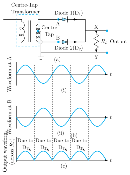
(a) Antimony makes Ge n-type (donor level near Ec) so conductivity rises; a p-n junction forms by diffusion then drift equilibrium; forward bias narrows and reverse bias widens the depletion layer. (b) A full-wave rectifier uses two diodes conducting on alternate half-cycles (output at 2f); the diode's asymmetric V–I curve makes it a one-way valve; carbon (Eg≈5.5 eV) is an insulator while silicon (Eg≈1.1 eV) is a semiconductor.
Part (a)
(i) Antimony-doped germanium
Antimony is pentavalent. Four of its valence electrons form covalent bonds with neighbouring Ge atoms; the fifth is very loosely bound and occupies a donor energy level Ed lying only ≈0.01 eV below the conduction-band edge Ec. At room temperature kBT≈0.026 eV easily ionises these donors, promoting electrons into the conduction band. The crystal becomes n-type (electrons are majority carriers), the electron density rises by orders of magnitude, and since σ=neμn+peμp with n≫p, the conductivity increases greatly; the Fermi level moves up close to Ec.
(ii) Formation of a p-n junction
- Diffusion: electrons (abundant in n) and holes (abundant in p) diffuse down their concentration gradients across the junction and recombine, leaving behind immobile ionised dopants — positive donor ions on the n-side, negative acceptor ions on the p-side. This charged, carrier-free region is the depletion layer.
- Drift: the exposed ions set up a built-in electric field (n → p) that pushes carriers back — a drift current opposing diffusion. Equilibrium is reached when drift current exactly cancels diffusion current, establishing the barrier (built-in) potential V0 (≈0.3 V for Ge).
(iii) Effect of biasing on depletion width
- Forward bias lowers the barrier to V0−V; the depletion layer narrows and a large forward current flows. …
Showing the 12 most recent of 21 on this concept.
- CBSE 2026Set 55/1/11 markMCQQ.In an unbiased p-n junction, at equilibrium, which of the following statements is true? (A) Diffusion current is zero but drift current exists. (B) Diffusion current exists but drift current is zero. (C) Diffusion and drift currents are equal and opposite. (D) Both the diffusion and drift currents exist but are unequal.
›Reveal solutionSolution
At equilibrium in an unbiased p-n junction, the net current is zero because the diffusion current (due to carrier concentration gradients) is exactly balanced by the drift current (due to the built-in electric field). The correct option is (C).
The core concept: Why two currents must cancel
A p-n junction at equilibrium means no external voltage is applied. Yet, inside the junction, two opposing processes are always active:
- Diffusion: Holes from the p-side (high concentration) diffuse into the n-side, and electrons from the n-side diffuse into the p-side. This creates a diffusion current in the direction of the concentration gradient.
- Drift: The diffusion of carriers leaves behind ionized dopant atoms (negative on the p-side, positive on the n-side), creating a built-in electric field across the depletion region. This field pushes carriers in the opposite direction — holes back to the p-side, electrons back to the n-side — producing a drift current.
At equilibrium, these two currents must exactly cancel. If they didn’t, there would be a net flow of charge, which would change the electric field until balance is restored. This is a fundamental consequence of the condition that the Fermi level is constant throughout the junction.
Watch outA common mistake is to think that at equilibrium, no currents exist at all. In reality, both diffusion and drift currents are present — they are just equal and opposite, so the net current is zero.
Step-by-step reasoning
-
Identify the equilibrium condition
An unbiased p-n junction has no external voltage source. The system is in thermodynamic equilibrium, meaning the Fermi level is flat (constant) across the entire device. This implies that the net current through the junction must be zero.
-
Recognize the two current components
The total current I across the junction is the sum of the diffusion current Idiff and the drift current Idrift:
I=Idiff+Idrift
Both are non-zero because there is a concentration gradient (driving diffusion) and a built-in electric field (driving drift).
- Apply the equilibrium constraint At equilibrium, I=0. Therefore: …
- CBSE 2026Set DS1 markMCQQ.In depletion layer of p-n junction diode, there are:i) only electronsii) only holesiii) both electrons and holesiv) neither electrons nor holes
›Reveal solutionSolution
The depletion region is depleted of mobile charge carriers — it contains only fixed ions.
Concept. When a p–n junction forms, electrons from the n-side diffuse across and recombine with holes on the p-side (and vice-versa). This leaves behind, near the junction, a thin region containing only the immobile positive donor ions (on the n-side) and immobile negative acceptor ions (on the p-side). Since the free electrons and holes have recombined/been swept away, this region h …
- CBSE 2026Set ANNUAL1 markMCQQ.The value of barrier potential for Si semiconductor is:(a) 0.3 V(b) 1.1 V(c) 0.7 eV(d) 0.7 V
›Reveal solutionSolution
The depletion-layer potential barrier that must be overcome to forward-bias a silicon diode is about 0.7 volt (compare germanium's ~0.3 V).
When a p-n junction forms, diffusion of majority carriers across the junction sets up a depletion region and an internal electric field, which corresponds to a potential difference — the barrier potential — that opposes further diffusion. For silicon this barrier potential is characteristically about 0.7 V (for germani …
- CBSE 2026Set ANNUAL1 markMCQQ.In P-n junction diode the width of depletion layer is :(a) 1 m(b) 1 μm(c) 1 nm(d) 1 pm
›Reveal solutionSolution
The depletion layer of a p-n junction is about 1 μm (≈10⁻⁶ m) wide.
When a p-n junction is formed, electrons and holes diffuse across the junction and recombine, leaving behind immobile ionised donor and acceptor atoms. This creates a region devoid of free charge carriers — the depletion layer.
…
- CBSE 2025Set IMPROVEMENT1 markMCQQ.The depletion layer of a p-n junction diode consists of:(a) Only holes(b) Only electrons(c) Both electrons and holes(d) Neither electron nor hole
›Reveal solutionSolution
The depletion layer is depleted of free charge carriers; it contains only fixed (immobile) ionised donor and acceptor atoms.
When a p-n junction is formed, free electrons from the n-side diffuse into the p-side and recombine with holes, and free holes from the p-side diffuse into the n-side and recombine with electrons, near the junction. This leaves behind immobile positively charged donor ions on the n-side and immobile negatively charged acceptor ions on the p-side, forming a narrow region called the depletion layer. This region is depleted of mobile …
- CBSE 2025Set ANNUAL1 markQ.A depletion layer consists of ................ . (fill in the blank)
›Reveal solutionSolution
The depletion layer at a p-n junction is a thin region stripped of mobile carriers, containing only fixed ionised donor/acceptor atoms.
When a p-n junction forms, free electrons near the junction on the n-side diffuse across and recombine with holes on the p-side (and vice-versa). This leaves behind, on either side of the junction, a narrow region of immobile ions: positively charged (uncompensated) donor ions on the n-side and negatively charged (uncompensated) acceptor ions on the p-side. This region is depleted of free (mobile) charge carriers — …
- CBSE 2025Set ANNUAL1 markMCQQ.Two statements are given below : one labelled as Assertion (A) and other labelled as Reason (R). Read the statements carefully and choose the correct option. Assertion (A) : The thickness of the depletion layer is fixed in all semi-conductor devices. Reason (R) : Free carriers are available in depletion layer.(a) Both Assertion (A) and Reason (R) are true and the Reason (R) is the correct explanation of Assertion (A).(b) Both Assertion (A) and Reason (R) are true, but the Reason (R) is the incorrect explanation of Assertion (A).(c) Assertion (A) is true, but Reason (R) is false.(d) Assertion (A) and Reason (R) both are false.
›Reveal solutionSolution
The depletion layer's thickness is not fixed (it changes with applied bias), and it contains no free carriers at all — both statements are wrong.
Assertion: False. The thickness of the depletion layer is not fixed — it changes with the applied voltage. Forward bias narrows the depletion layer (reduces the barrier), while reverse bias widens it (increases the barrier). It also depends on doping concentration.
…
- CBSE 2025Set ANNUAL1 markMCQQ.Assertion: Thickness of depletion layer is fixed in all semiconductor devices. Reason: No immobile charged carrier ions are available in depletion layer.(a) If both assertion and reason are true and the reason is the correct explanation of the assertion.(b) If both assertion and reason are true but reason is not a correct explanation of the assertion.(c) Assertion is true but reason is false.(d) Both assertion and reason are false.
›Reveal solutionSolution
The depletion layer's thickness is NOT fixed — it changes with applied bias — and the depletion layer DOES contain immobile ionised dopant ions, so both statements are false.
Assertion check: In a p-n junction, the depletion-region width depends on the applied voltage. Under forward bias, the width of the depletion layer decreases; under reverse bias, it increases; it also depends on doping concentration. So the assertion, that the thickness is 'fixed in all semiconductor devices', is FALSE.
…
- CBSE 2025Set ANNUAL1 markQ.What is the effect on the width of a depletion region of a p-n junction diode if the doping concentration is increased?
›Reveal solutionSolution
More dopant ions per unit volume means equilibrium (same barrier potential) is reached over a narrower depletion width.
The depletion region forms when majority carriers diffuse across the junction and leave behind fixed ionized dopant atoms. As doping concentration increases, there are more ionized dopant atoms per unit volume available near the junction, so the same total (equilibrium) amount of fixed charge — and hence the same barrier potential — is reached over a narrower region. So the width of the depletion region decreases as doping conc …
- CBSE 2025Set ANNUAL1 markMCQQ.The function of a rectifier is(i) to convert AC to DC(ii) to convert DC to AC(iii) both(i) and(ii)(iv) None of the above
›Reveal solutionSolution
A rectifier converts AC into DC.
A p-n junction diode conducts only when forward biased. In a rectifier this one-way behaviour allows current in only one direction during the AC cycle, so the pulsating output is unidirectional, i.e. direct current. Thus the function of a rectifie …
- CBSE 2024Set IMPROVEMENT1 markQ.Why do holes diffuse from p-region to n-region in an unbiased p-n junction?
›Reveal solutionSolution
Diffusion always moves majority carriers from a region of high concentration to low concentration.
In the p-region, holes are the majority carriers and are present in high concentration; in the n-region, holes are minority carriers, present in very low concentration. Whenever a p-n junction is formed, this large concentration gradient of holes across the junction drives them to diffuse from the p-region (high hole concentration) into the n-region (low hole concentration), exactly as any species diffuses from higher to lower concentration. (Similarly, electrons diffuse from the n-region into the …
- CBSE 2024Set A1 markMCQQ.In full wave rectifier, if input frequency is 50 Hz, then output frequency will be (A) 25 Hz (B) 50 Hz (C) 100 Hz (D) 200 Hz
›Reveal solutionSolution
A full-wave rectifier doubles the input frequency, giving 2 × 50 = 100 Hz → option (C).
In a full-wave rectifier, both halves of each AC input cycle are converted into output pulses of the same polarity. So for every one input cycle there are two output pulses, and the fundamental frequency of the rectified output is twice the input frequency:
…
🎓Unlock everything free for 14 days
- ✓Full step-by-step solutions
- ✓Concept-first explanations
- ✓Methods, shortcuts & mistakes
- ✓PYQ mapping + timed mock tests
Full access for 14 days. No credit card required.